


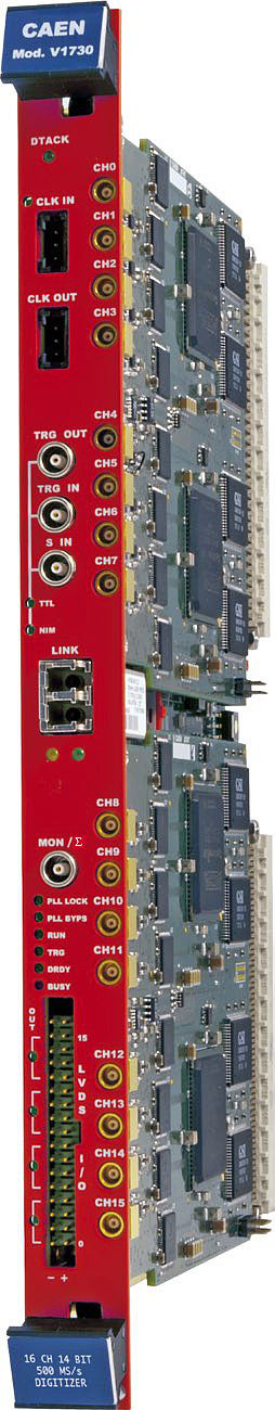
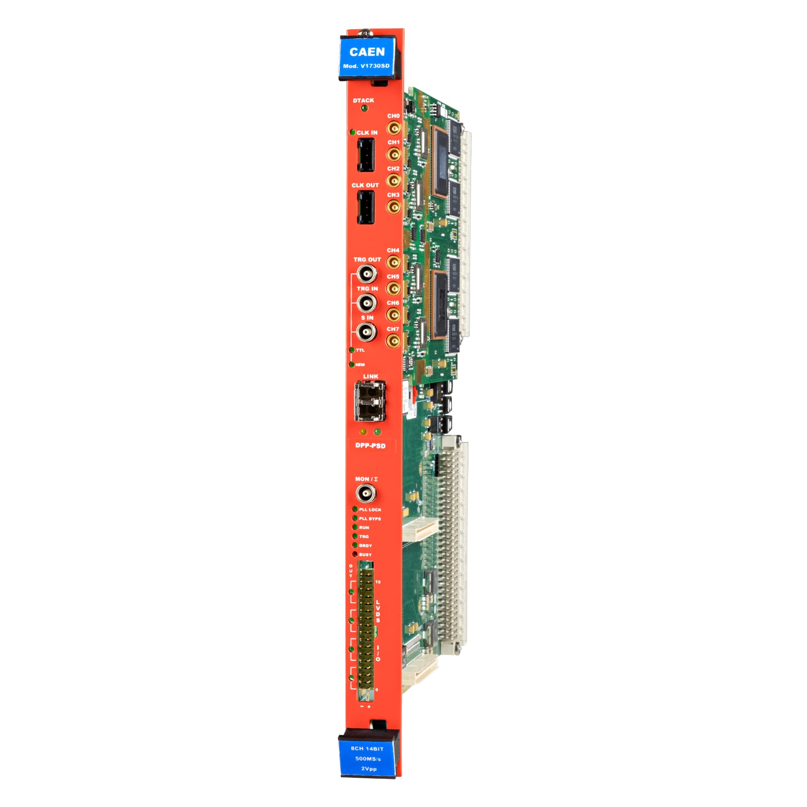
V1730 / V1730S
16/8 Channel 14 bit 500 MS/s Digitizer
Features
- 14-bit @ 500 MS/s
- Analog inputs on MCX coaxial connectors
- NSCLDAQ Supported (DPP-PSD and DPP-PHA only)
- 16/8 channels, 1-unit wide 6U VME64 module
- 0.5 and 2 Vpp selectable input dynamic range with programmable DC offset adjustment
- Algorithms for Digital Pulse Processing (Free Trial)
- VME64 (VME64X compliant) and Optical Link communication interfaces
- Multi-board synchronization features
- 16 programmable LVDS I/Os
- Daisy chain capability
- Compliant with CoMPASS, MC2Analyzer, DPP-ZLEplus and DPP-DAW Demo Software, C and LabVIEW libraries

Overview
The Mod. V1730S is a digitizer capable of recording waveforms along with performing advanced algorithms for online digital pulse processing (DPP) (Free Trial). Utilizing DPP Firmware, users can acquire quantitative physical parameters (Integrated Charge, Pulse Shape Discrimination with very fine time resolution, Pulse Height Analysis) as well as read out waveforms with automatic pulse identification and baseline suppression on channel basis (Zero-Length Encoding and Dynamic Acquisition Window). The wide range of DPP algorithms supported by the V1730S make it a “must-have” for any type of nuclear physics application.
The V1730S (previously V1730) has also been upgraded, introducing a larger FPGA to accommodate more complex DPP algorithms and a new A/D converter for better stability which does not require temperature-related calibration.
Input signals are read by a Flash ADC, 14-bit resolution and 500 MS/s sampling rate, which is well suited for mid fast signals as the ones coming from liquid or inorganic scintillators coupled to PMTs or Silicon Photomultipliers, but also for high precision detectors as Silicon or HPGe coupled with charged sensitive preamplifier. The acquisition can be channel independent and it is possible to make coincidence/anti-coincidence logic among different channels and external veto/gating. Multiple boards can be synchronized to build up complex systems. In the case of DPP mode, data can be saved in time-stamped list mode to support higher input rates and improving the throughput performances. Piled-up events can be rejected or saved for offline analysis. The acquisition in DPP mode is fully controlled by the CoMPASS and MC2Analyzer software, which manage the algorithm parameters, build the plots and saves the relevant energy, time, and PSD spectra. In the case of waveform recording mode, the user can take advantage of the CAENScope and WaveDump software to access and save the waveforms. Libraries and demo software in C and LabView are available for integration and customization of specific acquisition systems.
The V1730S comes in a VME form factor, with 16/8 input channels. The communication to and from the board is provided through the VMEBus and Optical Link interfaces.
Note: V1730 can be operated with VME8004B / VME8004X / VME8008B / VME8008X / VME8010 / VME8011 / VME8100 / VME8200. Never use this digitizer with crates VME8001, VME8002, VME8004 and VME8004A. Overheat may damage the module.
The V1730 fits in the single-slot CAEN VME64X u-crate, which allows you to convert the VME digitizer into a desktop board for lab tests.
Technical Specifications
- GENERAL
Form Factor: 1-unit wide, 6U VME64
Weight: 440 g (8 ch), 540 g (16 ch)
- ANALOG INPUT
Channels: 16/8 channels single ended
Bandwidth: 250 MHz
Impedance: 50 Ω
Connector: MCX
Full Scale Range: 0.5 or 2 Vpp (SW selectable)
Offset: Programmable DAC for DC offset adjustment in the full scale range
- DIGITAL CONVERSION
Resolution: 14 bits
Sampling Rate: 500 MS/s Simultaneously on each channel
- SYSTEM PERFORMANCES
V1730Sx Baseline RMS Noise (open inputs)
@ 2 Vpp: 2.6 LSB = 312 uV
@ 0.5 Vpp: 3.4 LSB = 102 uV
- ADC CLOCK GENERATION
Clock source: internal/external
Onboard programmable PLL provides generation of the main board clocks from an internal (50 MHz local Oscillator) or external (front panel CLK-IN connector) reference
- DIGITAL I/O
- CLK-IN (AMP Modu II)
AC coupled differential input clock LVDS, ECL, PECL, LVPECL, CML (single ended NIM/TTL available by CAEN adapter)
Jitter < 100 ppm requested
CLK-OUT (AMP Modu II)
DC coupled LVDS output clock for multi-board synchronizationTRG-OUT (LEMO)
Local trigger digital output
NIM/TTL, Rt = 50 Ω
TRG-IN (LEMO)
External trigger digital input
NIM/TTL, Zin = 50 ΩS-IN (LEMO)
SYNC/START front panel digital input
NIM/TTL, Zin = 50 Ω
- ACQUISITION MEMORY
- 640 kS/ch (1.25 ms @ 500 MS/s) or 5.12 MS/ch (10 ms @ 500 MS/s) Multi-event Buffer divisible into 1 ÷ 1024 buffers
- Independent read and write access
- Programmable event size and pre/post-trigger
- TRIGGER
- Trigger Source
Self-trigger: channel over/under threshold for either Common or Individual (DPP only) trigger generation
External-trigger: Common by TRG-IN connector
Software-trigger: Common by software command
Trigger Propagation
TRG-OUT digital outputTrigger Time Stamp
Waveform Recording: 31-bit counter, 16 ns resolution, 17 s range; 48-bit extension by firmware
DPP-PSD: 47-bit counter, 2 ns resolution, 78 h range; 10-bit and 2 ps fine time stamp with digital CFD
DPP-PHA: 47-bit counter, 2 ns resolution, 78 h range
DPP-DAW: 48-bit counter, 2 ns resolution, 156 h range
DPP-ZLEplus: 48-bit counter, 16 ns resolution, 625 h range
- SYNCHRONIZATION
- Clock Propagation
Daisy chain: CLK-IN/CLK-OUT connectors
One-to-many: clock distribution from DT4700 on CLK-IN connector
Clock Cable delay compensationAcquisition Synchronization
Sync Start/Stop through digital I/O (S-IN or TRG-IN input, TRG-OUT output)Trigger Time Stamp Alignment
By S-IN input connector
- ADC & MEMORY CONTROLLER FPGA
- x730
Altera Cyclone EP4CE30
(one FPGA serves 4 channels)x730S
Intel/Altera Arria V GX
(one FPGA serves 4 channels)
- ANALOG MONITOR
12-bit/125 MHz DAC FPGA controlled output with four operating modes:
- Test pulses: 1 Vpp ramp generator
- Majority signal: proportional to the no. of couples of channels under/over the threshold (steps of 125 mV)
- Memory Occupancy signal: proportional to the Multi-Event Buffer Occupancy (1 buffer ~ 1mV)
- Voltage level: programmable output voltage level
- LVDS I/O
- 16 general-purpose LVDS I/Os controlled by FPGA
- Busy, Data Ready, Memory Full, Individual Trg-Out and other functions can be programmed
- An Input Pattern from the LVDS I/Os can be associated to each trigger as an event marker
- COMMUNICATION INTERFACE
VME: VME 64X compliant. Data transfer mode: BLT32, MBLT64 (70 MB/s using CAEN Bridge), CBLT32/64, 2eVME, 2eSST (up to 200 MB/s)
Optical Link: CAEN CONET proprietary protocol, up to 80 MB/s transfer rate. Daisy chainable: it is possible to connect up to 8/32 ADC modules to a single Optical Link Controller (Mod.A2818/A3818)
- FIRMWARE
Waveform Recording Firmware: Free firmware for waveform recording
Upgrades: Firmware can be upgraded via Optical Link or VMEBus
DPP Firmware: Paid firmware for Digital Pulse Processing: DPP-PSD, DPP-PHA, DPP-ZLEplus, and DPP-DAW
- POWER CONSUMPTIONS
- V1730: 8.2 A @+5V; 840 mA @+12V; -12V not usedV1730B: 10.2 A @+5V; 840 mA @+12V; -12V not usedV1730C: 5 A @+5V; 400 mA @+12V; 400 mA @-12V (ref. PCB rev. 0)V1730D: 6.5 A @+5V; 400 mA @+12V; 400 mA @-12V (ref. PCB rev. 0)V1730SD: 6.3 A @+5V; 400 mA @+12V; -12V not usedV1730S: 9.3 A @ +5V; 900 mA @ +12V; -12 V not usedV1730SB: 11.5 A @ +5V; 800 mA @ +12V; -12 V not usedV1730SC: 5.3 A @ +5V; 500 mA @ +12V; -12 V not used
Compare
Compare with Digitizers.
Loading...
Accessories
- A654
- Cable assembly LEMO 00 male to MCX male – 1 m
- A659
- Cable assembly BNC male to MCX male – 1 m
- AI2700
- Optical Fiber Series
- A317
- Cable assembly for Clock distribution 3-pin AMPMODU IV female terminations – 18 cm / 25cm
- A318
- Adapter for Clock signal FISCHER S101A004 male to 3-pin AMPMODU IV female – 10 cm
- A316
- Cable assembly 2.54mm 2-pin header female - 5 cm
- A952
- Cable assembly 2.54mm 34 pin female to 2.54mm 34 pin female - 50 cm
- A953
- Cable assembly 2.54mm 34 pin female to two 2.54mm 34 pin female – 50 cm
- A954
- Cable assembly 2.54mm 34 pin female to two 2.54mm 16 pin female - 50 cm
Ordering Options
| Code | Description |
|---|---|
| WV1730BXAAAA | V1730B - 16 Ch. 14 bit 500 MS/s Digitizer: 5.12MS/ch, CE30, SE (Obsolete) RoHS |
| WV1730CXAAAA | V1730C - 8 Ch. 14 bit 500 MS/s Digitizer: 640kS/ch, CE30, SE (Obsolete) RoHS |
| WV1730DXAAAA | V1730D - 8 Ch. 14 bit 500 MS/s Digitizer: 5.12MS/ch, CE30, SE (Obsolete) RoHS |
| WV1730XAAAAA | V1730 - 16 Ch. 14 bit 500 MS/s Digitizer: 640kS/ch, CE30, SE (Obsolete) RoHS |
| WV1730SBXAAA | V1730SB - 16 Ch. 14 bit 500 MS/s Digitizer: 5.12MS/ch, Arria V GX, SE RoHS |
| WV1730SCXAAA | V1730SC - 8 Ch. 14 bit 500 MS/s Digitizer: 640kS/ch, Arria V GX, SE RoHS |
| WV1730SDXAAA | V1730SD - 8 Ch. 14 bit 500 MS/s Digitizer: 5.12MS/ch, Arria V GX, SE RoHS |
| WV1730SXAAAA | V1730S - 16 Ch.14 bit 500 MS/s Digitizer: 640kS/ch, Arria V GX, SE RoHS |
Related Products
Related Software
WaveDump2
Open Source Software for Digitizer 2.0 and 1.0 Series
WaveDump
CAEN Digitizer readout application
MC²Analyzer
Graphical software tool for digitizers running DPP-PHA firmware
Related Firmware
DPP-ZLEplus
Digital Pulse Processing for the Zero Length Encoding
DPP-SUP
Super Licence for CAEN Digitizers
DPP-PSD
Digital Pulse Processing for Charge Integration and Pulse Shape Discrimination