
-
32 channels, 14-bit @125 MS/s Digitizer
-
Handy Desktop form factor
-
Based on powerful Xilinx Zynq-7000 SoC with open FPGA
-
Fully supported by SCI-Compiler for easy FPGA programming (Firmware runtime license included onboard)
-
Ideally suited to readout PMTs and Position Sensitive detectors in R&D/Lab development stage
-
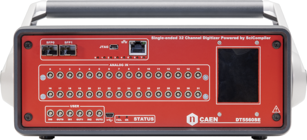
32 Single-ended analog inputs on LEMO connectors
-
Programmable analog frontend
-
[x1:x100] analog gain, adapting to many HEP and nuclear spectroscopy detectors
-
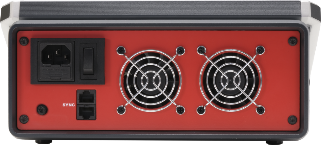
Board-to-board synchronization with a single CAT5e cable.
-
Configurable digital I/Os to interface with external systems
-
Maximum flexibility: USB2.0, Ethernet, and Optical Link (OPTIONAL) connectivity, to support remote management as well as extreme fast data flow
-
2.4” touch screen display for quick configuration and status control
-
Web Interface for quick board start-up
-
Default firmware for trapezoidal filter PHA and waveform recording
-
Open-source Open Hardware Readout Software
The CAEN Mod.DT5560SE is a Desktop, 32 Channel, 14-bit 125MS/s Waveform Digitizer which features an Open FPGA format which offers the user vast programmable data processing capabilities.
The DT5560SE Open FPGA Digitizer is ideally suited to readout detectors commonly used in HEP and nuclear spectroscopy, exploiting the handy form factor for R&D and prototyping in a laboratory. By taking advantage of the powerful SoC architecture the user can quickly and easily design custom logic and pulse processing algorithms on the open FPGA, as well as develop middleware/software which perfectly matches of the application of interest. No expertise in VHDL/Verilog is required for the user to utilize this powerful tool.
The board can simultaneously manage digital (LVDS, NIM, TTL) and analog signals, thus supporting the implementation of a wide range of functionalities required by physics experiments: Signal Digitization, Complex Trigger Logic, Pulse Height Analysis with MCA capabilities, Time Tagging, Pulse Shape Discrimination, etc. The DT5560 features single-ended analog inputs on LEMO connectors and an advanced programmable input stage with different possible gain and offset, suitable to adapt to a wide range of detectors.
Critical to the DT5560SE design is an open-FPGA architecture. Thanks to SCI-Compiler software, users can combine several processing blocks in a block diagram, supporting the quick and simple development of firmware algorithms critical to data processing. In few clicks, and without the knowledge of any FPGA programming language, it is possible to implement Pulse Height Analysis (PHA), highly accurate event timing and timestamping (TDC), mathematical operations (including data fitting), Pulse shape discrimination (PSD), and much more.
Free and open-source SCI-55×0 readout software is also provided. This open-source demo software is designed to manage the standard pulse height analysis firmware implementing energy measurements using a trapezoidal filter together with waveform recording.
Developed in collaboration with Nuclear Instruments.
You also may be interested in…
Request a Quote

Technical Specifications

|
General |
Form Factor: Desktop 257 x 102 x 331 mm3 (WxHxD) |
||||
|
Analog Input |
Channels: 32 single-ended inputs on LEMO Impedance: 50 Ω/1 kΩ programmable Bandwidth: 60 MHz, Programmable DC offset adjustment on each input in the full scale range Analog Coarse Gain: [x1:x100] Full Scale Range: [0.015 Vpp: 1.5 Vpp] |
||||
|
Digital I/Os |
USER IO 0…2 (LEMO)
|
||||
|
Digital Conversion |
|
||||
|
Clock Generation |
125 MHz ADC clock Clock sources: internal/external Internal 25 MHz oscillator External 25 MHz – USER IN 0 or SYNC connector |
||||
|
Trigger |
|
||||
|
Synchronization |
Clock Propagation: USER I/Os connectors SYNC Connector Acquisition Synchronization
Sync connector allows to cascade multiple units and synchronize them with a single standard CAT5e cable |
||||
|
FPGA |
Open FPGA: Xilinx Zynq-7000 SoC Z-7030 |
||||
|
Memory |
|
||||
|
Communication Interface |
The different readout interface allows to integrate the DT5560SE in existing experimental environment.
|
||||
|
Firmware |
Default
Custom
|
||||
|
Firmware Upgrade |
Firmware can be upgraded via Ethernet, mini-USB or JTAG mini-USB debugger (on-the-fly) |
||||
|
Software |
|
||||
|
Power Requirements |
|
Footer

