
Highlights
-
Positive or negative input signals
-
Energy sensitivity range of 5, 30 or 60 mV/MeV (Si)
-
Low noise
-
Timing output
-
Up to 5 kV (positive or negative) detector bias voltage
Overview
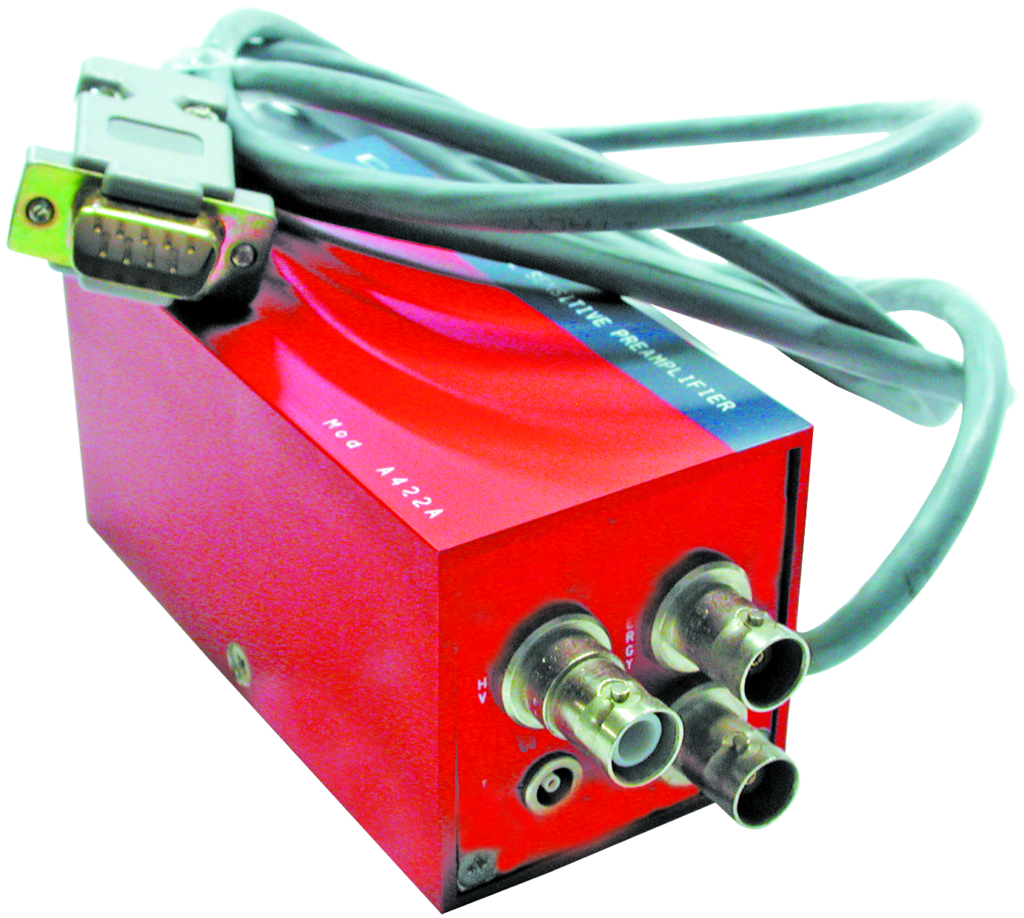
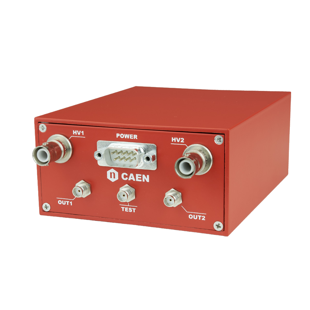
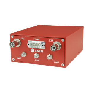
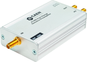
The CAEN Mod. A422A is a charge sensitive preamplifier, designed to be used especially with semiconductor detectors and in particular whenever the charge division is required (as in position sensitive silicon detectors). The unit accepts both positive and negative input pulses. A Test input for detector gain calibration and a HV input (up to 5 kV) for the detector bias are also included.
The output is an inverting unipolar voltage pulse, proportional in amplitude to the integrated charge; decay time is 300 µs. A Timing output provides an unipolar inverting fast voltage pulse, with a 15 ns typical rise time, across a 50 Ω load. Three different sensitivities (5, 30 or 60 mV/MeV) can be selected.
You also may be interested in…
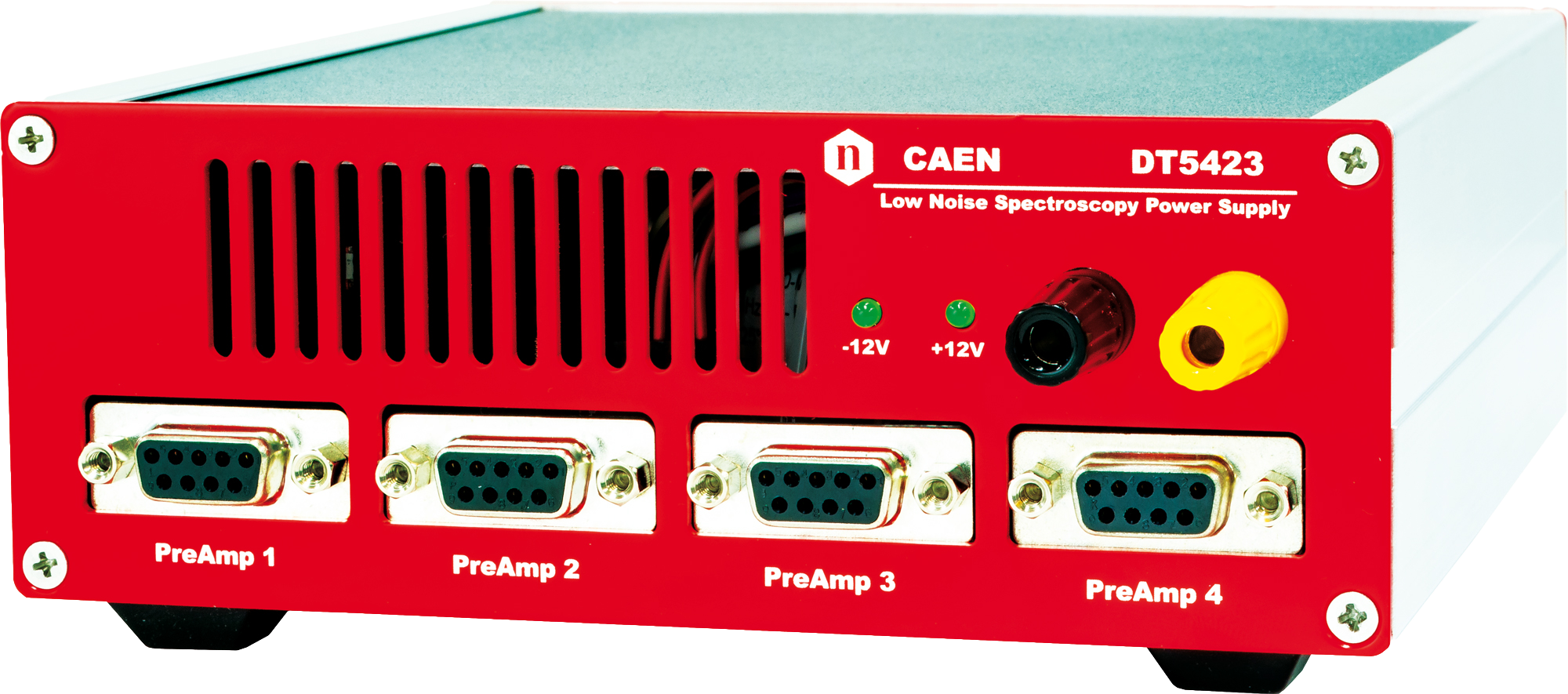
DT5423
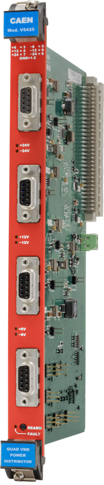
V5425
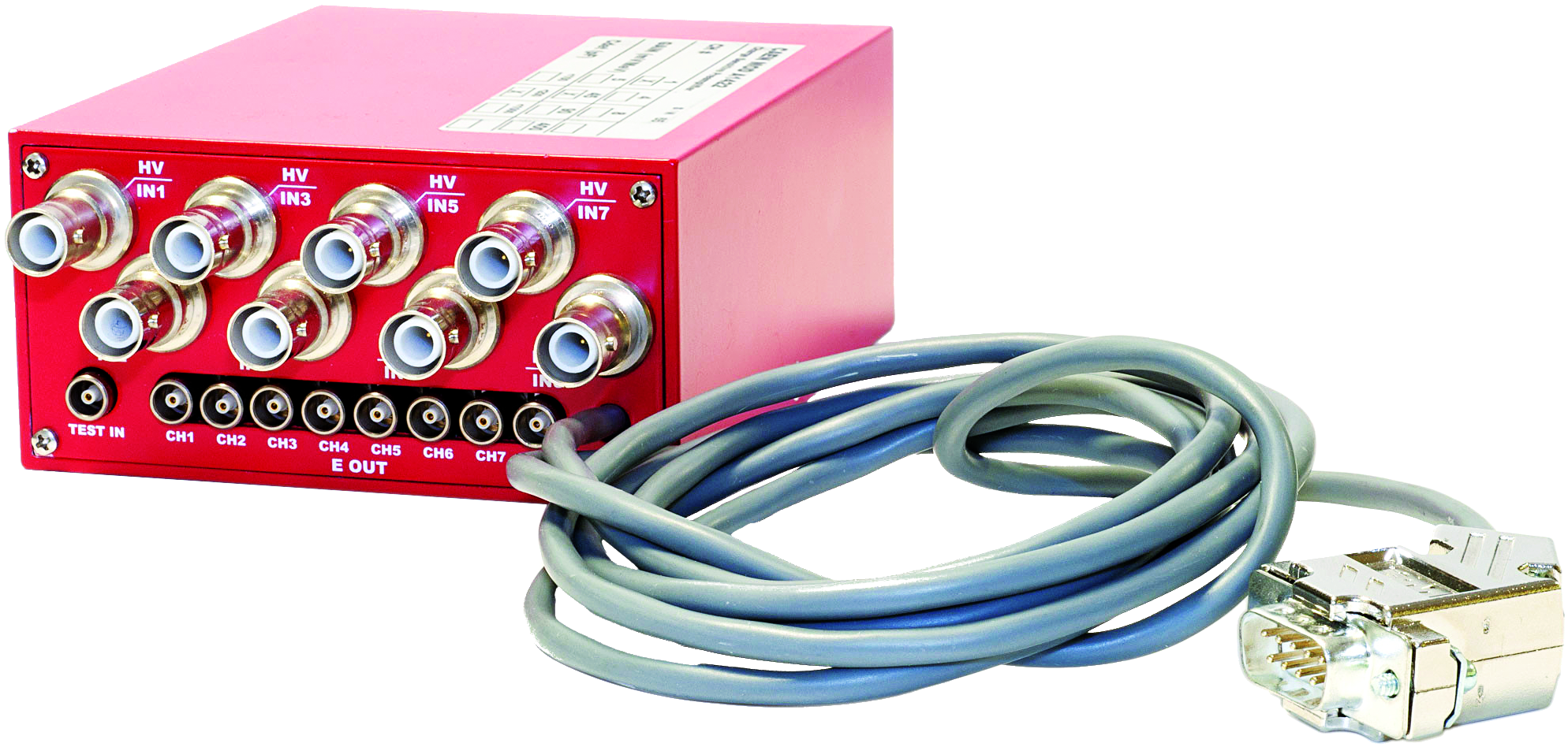
A1422
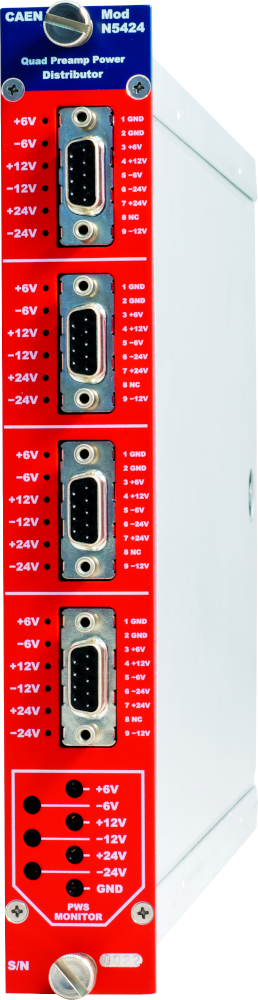
N5424
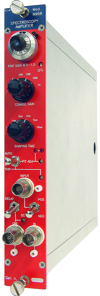
N968
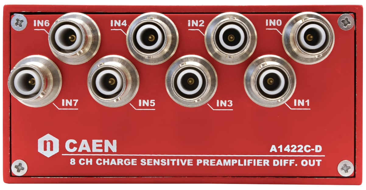
A1422C/D
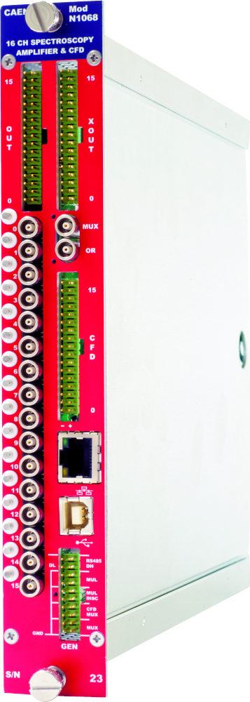
N1068
A1422E/F
Request a Quote

Compare

|
Image
|
Name
|
Package
|
Out Conn.
|
In Conn.
|
Test Capac. (pF)
|
Max Detector Bias Voltage (V)
|
Integral Non-linearity
|
Output Linear Range (V)
|
Output Rise Time (ns)
|
Noise FWHM keV (Si)
|
Sensitivity (mV/MeV) (Si)
|
No. Of Channels
|
|
|
A1422H |
15 Pin SIP hybrid |
- |
- |
1 / 10 / 47 |
±800 |
< ± 0.05% (0 ÷ ±10 V 1 kΩ term.) |
±10 (1 kΩ term.) ±4.5 (50 Ω term.) |
< 5/10/70 @0pF <20/25/45 @390pF |
< 2.2/4.7 @0pF <5.8/10.5 @390pF |
1/5/45/90/<br>400/450 |
1 |
|
|
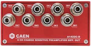
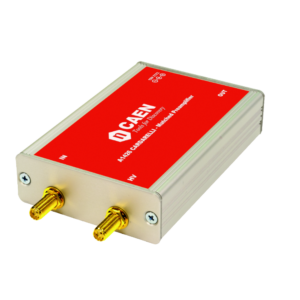
A1422C/D |
Shielded box |
RJ-45 |
SHV |
1 / 10 |
± 2000 |
<± 0.05%<br>(0 ÷ ±10V 1 kΩ term.) |
±5 (1 kΩ term.)<br>±2.5 (100Ω term.) |
< 5 @0pF<br><15 @200pF |
< 4.7 @0pF<br>< 7.6 @200pF |
5 |
8 |
|
|
A1422 |
Shielded box |
LEMO or BNC |
SHV |
1/10/47 |
±2000 |
< ± 0.05% <br>(0 ÷ ±10V 1kΩ term.) |
±10 (1kΩ term.)<br>±4.5 (50Ω term.) |
<5/10/70 @0pF<br><10/20/25/45 @390pF |
<2.2/4.7 @0pF<br><5.5/5.8/10.5/36 @390pF |
1/5/45/90/<br>400/450 |
1/4/8 |
|
|
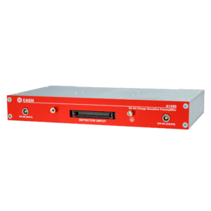
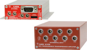
A1429 |
Shielded box |
Header (17+17) |
Samtec 80-pin 0.8mm |
0.5 / 1 / 2.2 |
±400 V Max |
N.A. |
Differential ± 4.5 VDiff max on 100Ω Term |
<20ns @0 pF<br><60ns @200 pF |
<5 KeV @0 pF<br><35 eV/pF |
20/45/90/<br>200/400 |
64 |
|
|
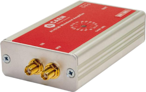
A1422E/F |
Shielded box |
SMA |
SMA |
1 |
±750 |
<±0.05%<br>(0 ÷ ±10V 1kΩ term.) |
±10 (1 kΩ term.)<br>±4.5 (50 Ω term.) |
<5.4 @0pF<br><60 @330pF |
<2.8 @0pF<br><6.8 @330pF |
200 |
2/4 |
|
|
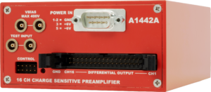
A1442 |
Shielded box |
Header (17+17) |
D-SUB 25 |
N.A. |
±400 |
N.A. |
Differential ±4.5 Vdiff |
< 10 @0pF<br /><20 @200pF |
<5 @0pF<br><9.5 @200pF |
20 / 100 <br>Selectable |
16/32 |
|
|
Discontinued A422 |
14 pin SIP hybrid |
- |
- |
10 |
±1000 |
<0.05% |
± 8 ± 4 |
<20 |
<9.8 @470pF |
1/45/90 |
1 |
|

|
A422A |
Shielded box |
BNC |
SHV |
10 |
±5000 |
< 0.045% |
± 8 ± 4 |
< 50 |
<17.5 @1nF |
5/30/60 |
1 |
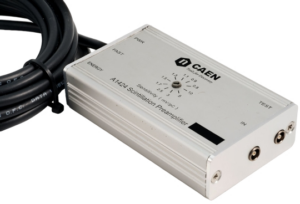
Technical Specifications
|
Packaging |
Alloy box: 100 mm x 50 mm x 50 mm |
|
Input Signals (IN/DETECTOR) |
SHV; accepts positive and negative charge pulses from semiconductor detectors and supplies the HV bias to the detector itself. * Output tested by using an input pulse with 50 ns rise time and a 1000 µs fall time. |
|
Input Signals (HV) |
SHV; up to 5 kV (positive or negative) for the detector bias. 101 MΩ resistance in series |
|
Input Signals (TEST) |
LEMO 00; positive or negative inputs to calibrate the gain of the detector input via Ctest = 10 pF |
|
Output Signals (OUT/ENERGY) |
BNC; inverting unipolar voltage pulse proportional in peak amplitude to the charge input. DC offset adjustable to zero via the internal R12 trimmer. 50 ns minimum rise time, 300 μs decay time, ±8 V max. peak amplitude |
|
Output Signals (TIMING) |
BNC; inverting unipolar fast voltage pulse. 14 ns minimum rise time. Requires a 50 Ω termination whether it is used or not. |
|
Integral non linearity |
± 0.045% (from 0 to ± 8 V peak output) |
|
Gain drift |
< ± 50 ppm/°C to (from 0° to 50°C) |
|
Energy sensitivity |
60/30/5 mV/MeV (Si) selectable via internal jumpers (± 10%) |
|
Typical noise |
17.5 KeV FWHM at 1000 pF capacitance and 60 mV/MeV sensitivity |
|
Power Requirements |
|
Footer