Highlights
-
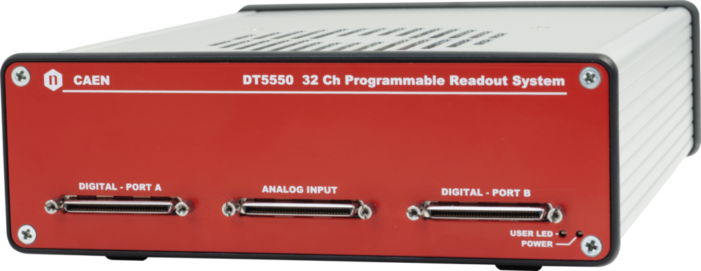
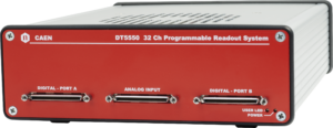
32-channel Sequencer and Readout System (fully differential inputs)
-
Integrated system for managing digital and analog ASIC outputs
-
Ideally suited for R&D projects involving ASICs with multi-channel detectors
-
48 differential digital lines and 2A power supply to support ASICs readout
-
Multi-board support for system-building
-
Optional Digitizer functionality via DT5550AFE (single-ended analog inputs) accessory
-
80MS/s, 14bit ADC
-
USB 3.0 for fast data transfer
-
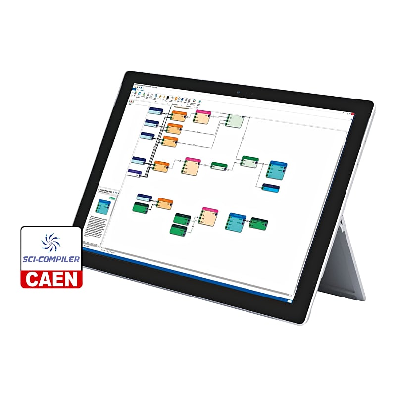
“Open-FPGA Capability” via Sci-Compiler software, a graphical development platform for quick, user-friendly FPGA programming
-
Dramatically simplifies development of complex logic schematics and processing algorithms
-
Automatic VHDL firmware code generation via GUI-based block diagrams
-
Supports processing functions such as PHA-based Trapezoidal Filter, Peak Stretcher, Charge Integration, Waveform Recording, MCA, Scaler, and more…
-
-
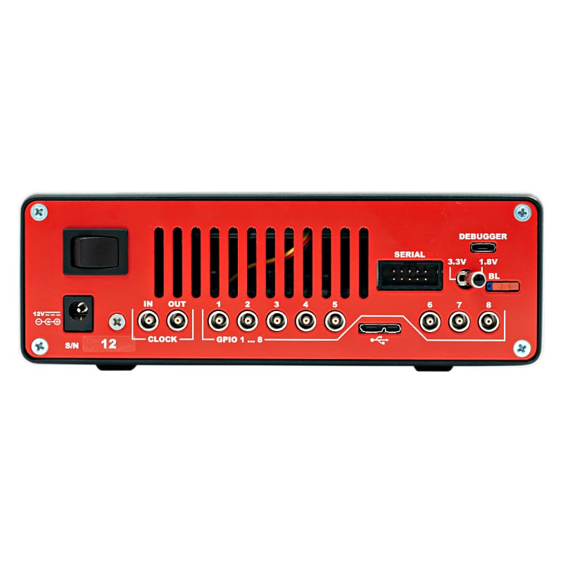
8 programmable digital I/O on LEMO connectors for external control signals (trigger, veto, busy, etc…)
-
Standard VHDCI Connectors
-
1 analog connector with 32 analog channels and an I2C bus
-
2 digital connectors carrying 24 differential digital lines (each) and programmable power supply for ASICs control”
-
Overview
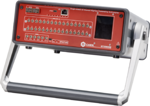
The CAEN Mod. DT5550 is a Programmable 32-channel Sequencer and Readout System for physics application. It is one of the CAEN programmable board compatible with SCI-Compiler, the innovative software tool for easy FPGA programming, designed to help users in building a customized DAQ. The default firmware, the demo readout software and some design files are distributed for free and open source, allowing the user to minimize the effort in designing the DAQ.
The DT5550 is capable to manage simultaneously a large number of digital and differential analog signals, making it suitable to readout most of the ASICs commonly used in physics applications.
The DT5550 is fully supported by SCI-Compiler, a Windows-based graphical development system for block-diagram-based FPGA programming. This tool allows to develop and compile the firmware code using graphical blocks which represents the functionalities needed for firmware implementation (for example oscilloscope, TDC, MCA, charge integration, etc). SCI-Compiler automatically generates the VHDL firmware code starting only from logic blocks and virtual instruments that can be connected together in the GUI and, moreover, it generates C/C++/C#/Python Libraries for custom software development in Windows and Linux.
A complete, ready to use default firmware is provided for free and open source. The default firmware manages the basic waveform digitization and charge integration and it is preloaded on the board. The user can open the default firmware in SCI-Compiler and modify it in order to customize, for example, the trigger logic, the data online processing or integrate it in a larger system.
The SCI-Compiler license and one-year free upgrade is included with the DT5550.
The SCI-55×0 Readout Software is the free and open source Windows-based software developed to perform basic acquisitions with the DT5550. It works in conjunction with the DT5550 default firmware and it can be modified by the user according to the custom functions implemented in the firmware and for any other need.
Available board models and accessories are listed in the tab “ordering option” and “accessories”.
Developed in collaboration with Nuclear Instruments.

You also may be interested in…
Request a Quote

Compare

|
Image
|
Name
|
Analog Input
|
Connectors
|
Detector Frontend
|
Power Supply for Detector
|
Sampling Rate
|
Programmable Digital I/Os
|
Open FPGA
|
Communication Interface
|
Touchscreen Display
|
Readout Software
|
SCI-Compiler Software
|
Form Factor
|
|
|
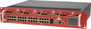
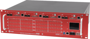
New R5560 |
128 |
RJ45 |
No |
No |
14-bit @ 125 MS/s |
128 + 6 |
Xilinx Zynq-7000 SoC |
USB 3.0, Optical Link, Ethernet |
Yes |
Yes |
Included |
Rack |
|
|
New R5560SE |
128 |
MCX |
Programmable |
No |
14-bit @ 125 MS/s |
128 + 6 |
Xilinx Zynq-7000 SoC |
USB 3.0, Optical Link, Ethernet |
Yes |
Yes |
Included |
Desktop |
|
|
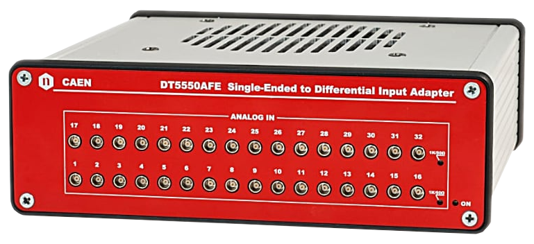
DT5550 |
32 |
VHDCI |
DT5550AFE available for single-ended detectors |
No |
14-bit @ 80 MS/s |
48 |
Xilinx Kintek-7 |
USB 3.0 |
No |
Yes |
Included |
Desktop |
|
|
DT5560SE |
32 |
LEMO |
Programmable |
No |
14-bit @ 125 MS/s |
32+ 6 |
Xilinx Zynq-7000 SoC |
Micro-USB, Optical Link, Ethernet |
Yes |
Yes |
Included |
Desktop |
|
|
DT5550W |
Up to 128 |
Input for SipM |
Weeroc ASIC |
20 - 85 V |
ASIC internal ADC or external ADC 14-bit @ 80 MS/s |
8 |
Xilinx Kintek-7 |
USB 3.0 |
No |
Yes |
Included |
Desktop |
Technical Specifications
|
Packaging |
163 x 50 x 226 mm3 (WxHxD) Desktop |
|
Analog Input |
Channels: 32 Channels, Differential |
|
Digital Input |
Channels: 2 x 24 channels, Differential |
|
Digital Conversion |
Resolution: 14 bits |
|
Clock Generation |
Clock source: internal/external |
|
LEMO Digital I/O |
CLOCK-IN (LEMO) CLOCK-OUT (LEMO) GPIO 1 – 8 (LEMO) |
|
Memory |
16 kS/ch |
|
Trigger |
Trigger Source Trigger Propagation Trigger Time Stamp |
|
Synchronization |
Clock Propagation Acquisition Synchronization |
|
FPGA |
Open FPGA |
|
Communication Interface |
USB 3.0 |
|
Firmware |
Default: Waveform recording and Charge Integration Custom: Use SCI-Compiler to develop your own firmware (LICENSE INCLUDED) |
|
Firmware Upgrade |
Firmware can be upgraded via USB 3.0 or mini-USB debugger (on-fly) |
|
Software |
|
Footer