
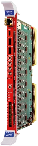
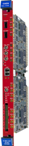
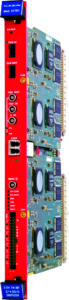
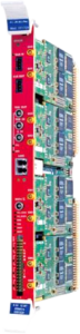
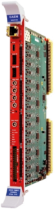
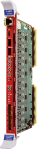
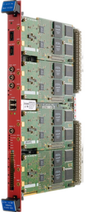
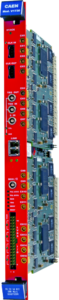
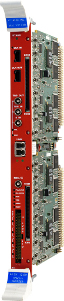
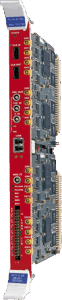
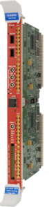
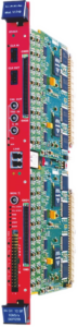
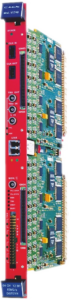
V2745
64 Channel 16 bit 125 MS/s Digitizer with Programmable Input Gain
Highlights
-
16 bit @ 125 MS/s ADC
-
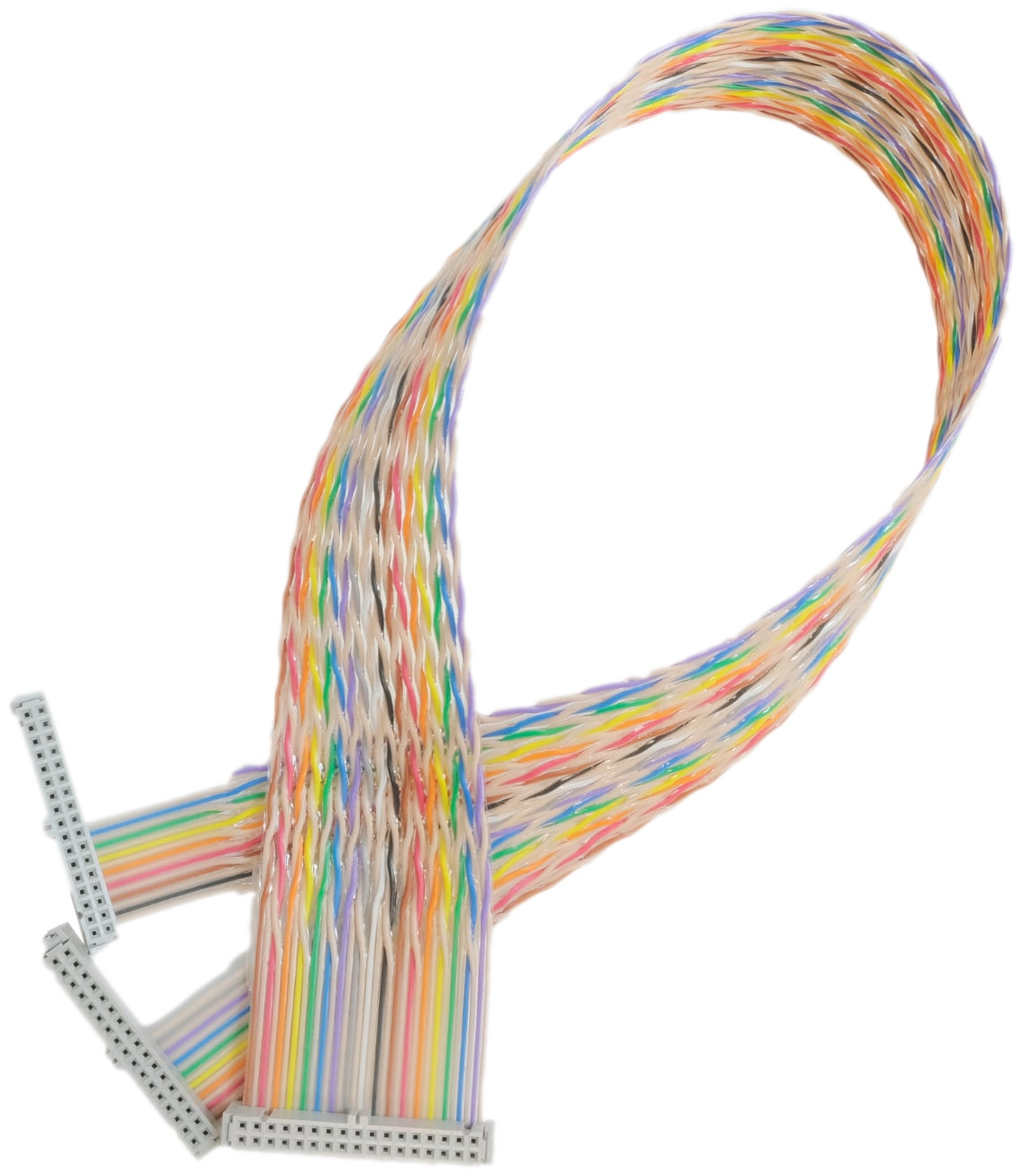
64 analog inputs, differential or single-ended, on four 2mm 40-pin header connectors
-
Software selectable Analog Gain up to x100
-
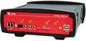
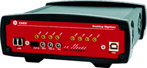
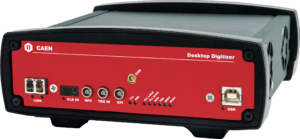
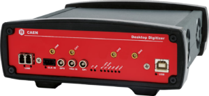
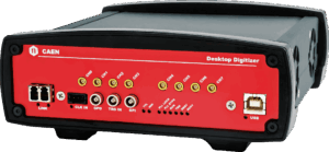
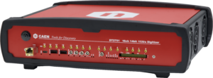
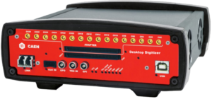
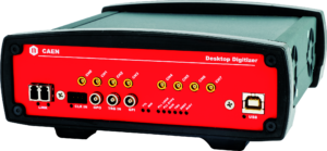
DT2745 desktop form factor also available
-
Open FPGA programming through graphical tool SCI-Compiler
-
Wide range of applications (from Neutrino Physics & Dark Matter to Nuclear and Particle Physics to Spectroscopic Imaging)
-
Suited for signals from Semiconductor Detectors coupled with CSPs (Si, HPGe) or scintillators coupled with PMTs (NaI, CsI)
-
On-board firmware selection for different acquisition modes:
-
Scope mode (simultaneous raw waveform acquisition on common trigger)
-
DPP-PHA mode (pulse height and time acquisition on independent channel self-triggers)
-
DPP-PSD mode (pulse shape discrimination and time acquisition on independent channel self-triggers)
-
Predisposition for other algorithms like zero suppression and data reduction
-
-
Multi-board synchronization and system building capabilities
-
Front panel fully programmable I/Os (4 LEMO TTL/NIM and 16 LVDS)
-
Special 125MS/s 14bit DAC output (LEMO) for signal inspection or trigger sum
-
On-board Xilinx Zynq® UltraScale+™ FPGA with embedded Linux-based ARM processor
-
2.5GB of Total Acquisition memory (DDR4)
-
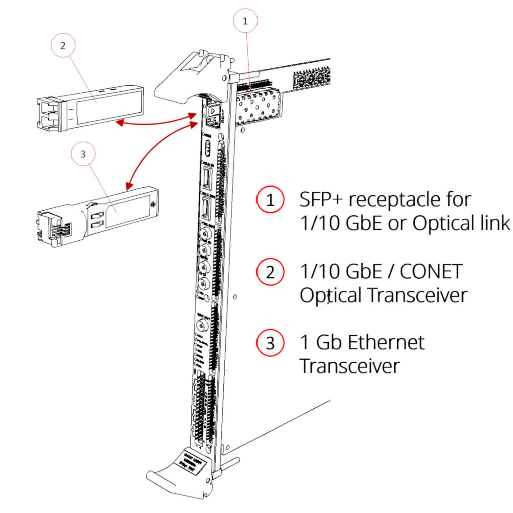
Multi Interface: USB-3.0 and 1/10 GbE or CONET optical link (switchable on the same socket)
-
SDK for embedded Arm and host PC
-
Open FPGA
Overview
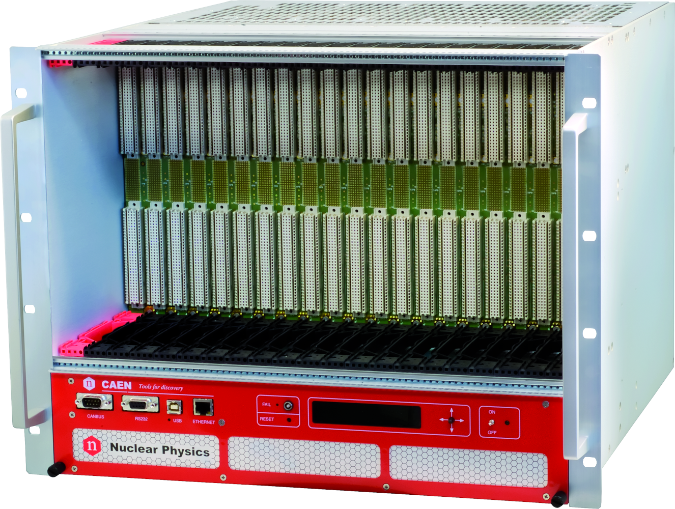
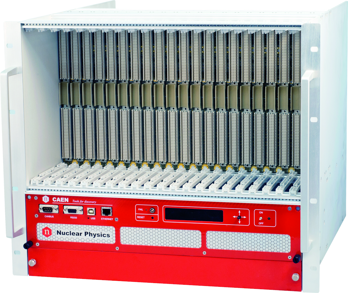
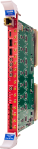
The Mod. V2745 Digitizer is a 64-channel digital signal processor for radiation detectors in a VME64X form factor. It offers not only waveform digitization and recording but also Multi-Channel Analysis for nuclear spectroscopy using Silicon strip, segmented HPGe, Scintillation detector with PMTs, Wire Chambers, and others.
The V2745 can perform pulse height measurements (PHA), and other algorithms that will be gradually developed, such as constant fraction timing (CFD), charge integration (QDC) and pulse shape discrimination (PSD). Algorithm settings can be set independently channel by channel.. The input channels with software selectable analog gain up to x100 are provided as differential (on V2745 versions) or single-ended (on V2745B version).
Each channel of the module digitizes the analog input, that can be the signal coming from a physics detector, with a 16 bit, 125 MS/s ADC. The sampled data are used to initiate the digital pulse processing sequence, managed in the FPGA at the firmware level. Different firmware types can be selected via software, according to the specific setup and acquisition mode.
-
Common trigger: all channels acquire simultaneously with a common trigger. The trigger can be fed externally or generated by a combination of individual channel discriminators. This mode is mainly intended for the acquisition of waveforms, like a digital oscilloscope. Options for zero suppression are available to remove not significant data.
-
Independent trigger: suited for trigger-less applications, where no global trigger is needed but each channel acquires waveforms upon its self-trigger which fires through a digital discriminator, independently of the others.
-
DPP: real-time processing in the FPGA allows for the extraction of physical parameters from the waveform (e.g. pulse height, charge, timestamp, PSD), well suited for high counting rate applications. It is yet possible to save both raw waves and parameters.
A template of the firmware is available for customers who want to personalize the acquisition to implement custom algorithms for pulse processing in the open FPGA. The user can have control of the data output information and customize the trigger logic to get several combinations of self-triggers and I/O signals to validate or discard the events.
Custom software can run on the onboard CPU for data reduction and analysis. Multi-board synchronization can be implemented via backplane or front panel easy-cabling options.
The communication interface selection offers fast readout options: USB 3.0 type-C and 1/10 Gigabit Ethernet or optional Optical (CONET – CAEN Daisy Chainable Optical Link Protocol Available on request) Links.
Supported third-party software:
The V2745 fits in the single-slot CAEN VME64X u-crate, which allows you to convert the VME digitizer into a desktop board for lab tests.
Moreover, you can check this FAQ to see which CAEN VME crates are suitable for this product.
Software

CAEN Toolbox

COMPASS
Sci-Compiler
Graphical Programming Language for CAEN Open FPGA Boards

WaveDump
Readout Application for CAEN Digitizer 1.0

CAEN FELib Library


Accessories
A954
A316
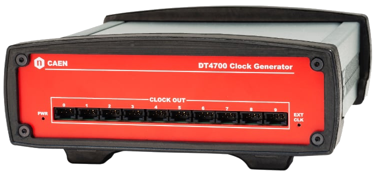
DT4700
A319A
A319B
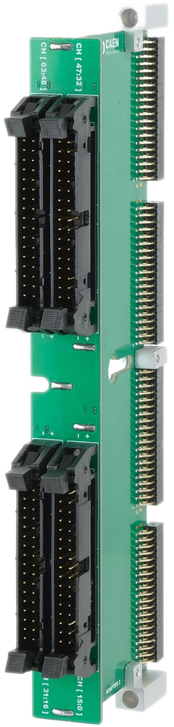
A372F
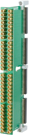
A372M
A952
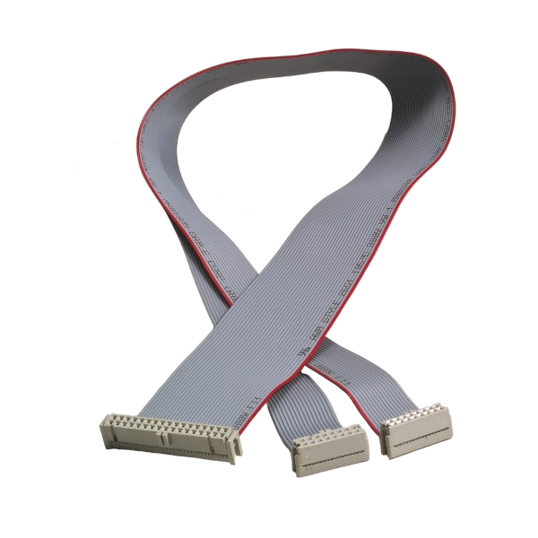
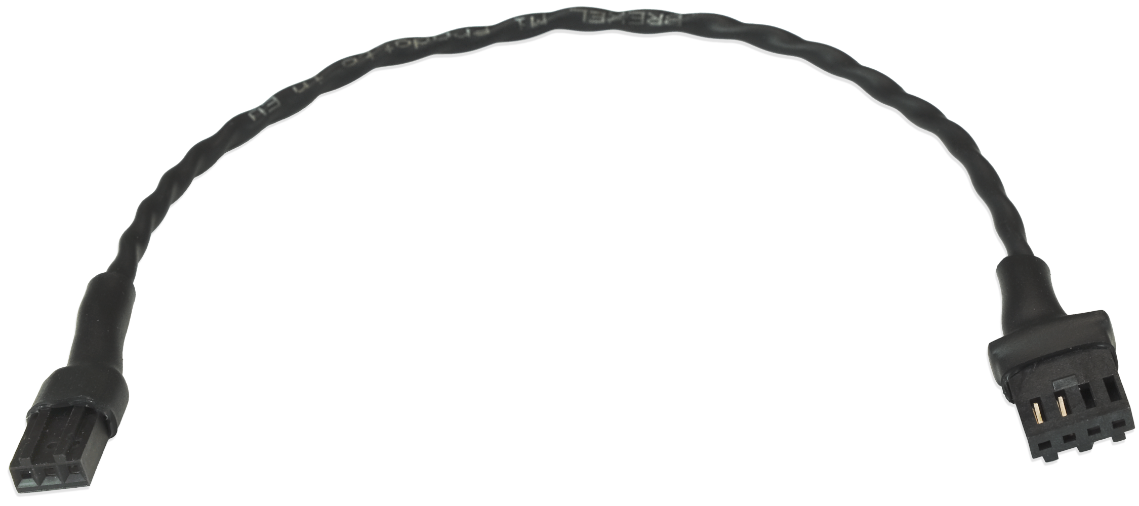
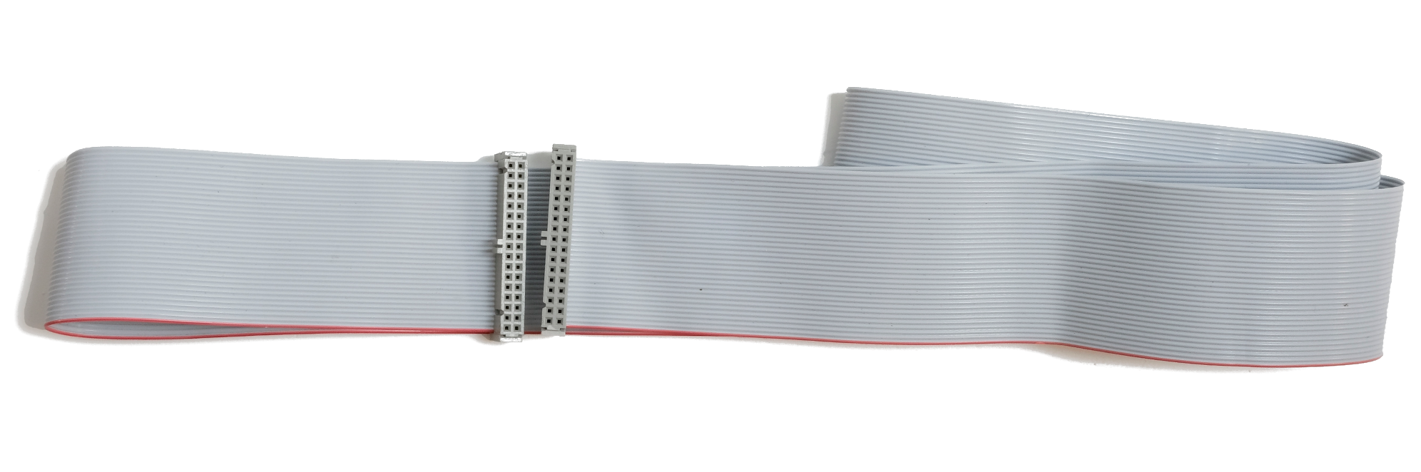
Cable assembly 2.54mm 34 pin female to 2.54mm 34 pin female - 50 cm
A953
Cable assembly 2.54mm 34 pin female to two 2.54mm 34 pin female – 50 cm
You also may be interested in…
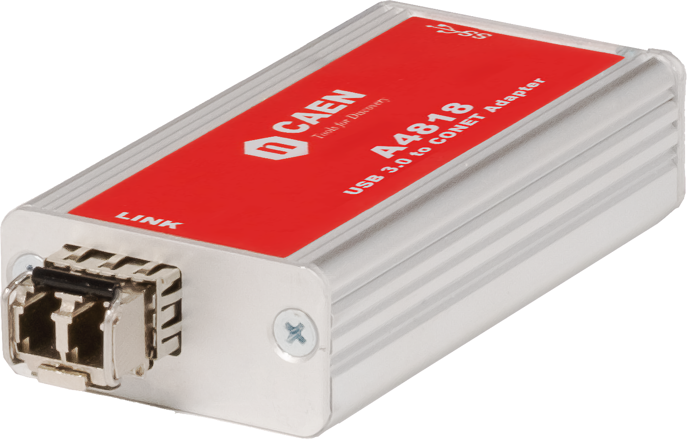
A4818
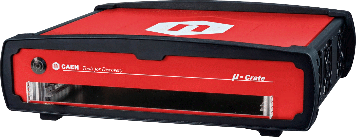
µ-crate
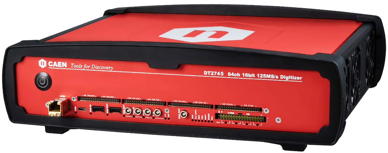
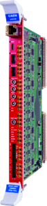
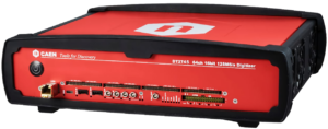
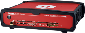
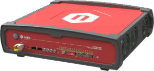
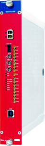
DT2745
VME8100
VME8200
A5818
VX2745
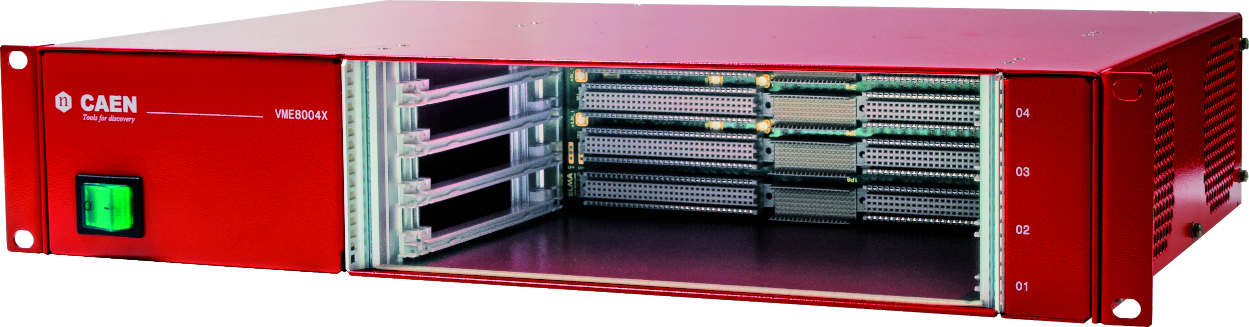
VME8004X
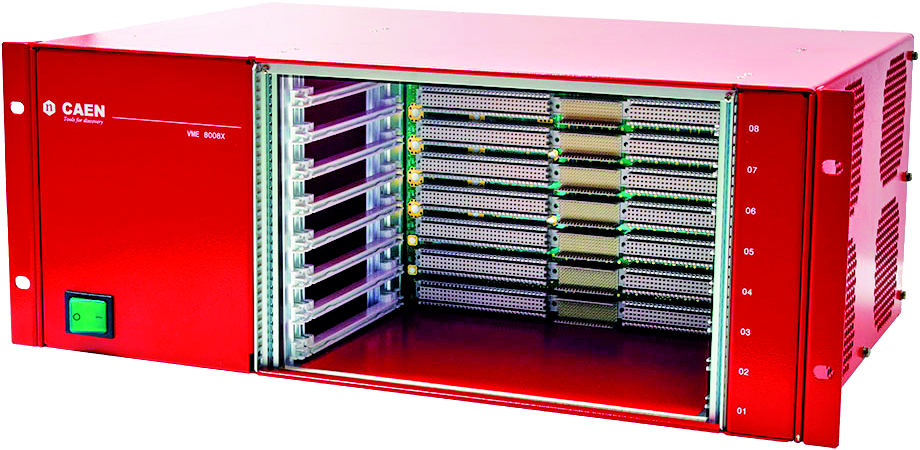
VME8008X
Request a Quote

Compare

|
Image
|
Name
|
Package
|
No. of Channels
|
Max Sampling Rate (MS/s)
|
Bandwidth (MHz)
|
Full Scale Range (V)
|
Resolution (bits)
|
Board Memory (Samples/ch)
|
Analog Input Connectors
|
CAEN firmware
|
Open FPGA
|
|
|
VX2730 |
VME64X |
32 |
500 |
250 |
[0.2 ÷ 4] |
14 |
84 M |
MCX |
DPP-PHA, DPP-PSD, D-SCOPE (cs) |
YES |
|
|
V1725 / V1725S |
VME |
8 / 16 |
250 |
125 |
0.5 - 2 |
14 |
640 k / 5.12 M |
MCX |
DPP-PHA, DPP-PSD, DPP-ZLEplus, D-WAVE |
NO |
|
|
DT2745 |
Desktop |
64 |
125 |
20 |
[0.04 + 4] |
16 |
21 M |
2mm 40-pin header male |
DPP-PHA, DPP-PSD, D-SCOPE, DPP-ZLEplus<sup>(cs)</sup> |
YES |
|
|
New R5560 |
rack mount 19 -2U |
128+6 |
125 |
60 |
2 |
14 |
max. 8k |
RJ45 |
n. a. |
YES |
|
|
New DTL2730 |
Desktop |
8 |
500 |
TBD |
TBD |
14 |
TBD |
MCX |
DPP-PHA(cs), DPP-PSD(cs), D-SCOPE(cs) |
YES |
|
|
V1761 |
VME |
2 |
4000 |
1000 |
1 |
10 |
7.2 M / 57.6 M |
MCX |
D-WAVE |
NO |
|
|
DT5751 |
Desktop |
2(DES mode) - 4 |
2000(DES mode) - 1000 |
500 |
0.2 / 1 |
10 |
3.6 M(DES mode) - 1.8 M |
MCX |
DPP-PSD, DPP-ZLEplus, D-WAVE |
NO |
|

|
VX1740D |
VME64X |
64 |
62.5 |
30 |
2 / 10 |
12 |
192 k |
SMC 68P |
DPP-QDC, D-WAVE |
NO |
|
|
DT5725 / DT5725S |
Desktop |
8 |
250 |
125 |
0.5 - 2 |
14 |
640 k / 5.12 M |
MCX |
DPP-PHA, DPP-PSD, DPP-ZLEplus, DPP-DAW, D-WAVE |
NO |
|
|
VX1724 |
VME64X |
8 |
100 |
40 |
0.5 / 2.25 / 10 |
14 |
512 k / 4 M |
MCX |
DPP-PHA, DPP-DAW |
NO |
|
|
DT5761 |
Desktop |
1 |
4000 |
1000 |
1 |
10 |
7.2 M |
MCX |
D-WAVE |
NO |
|
|
VX2745 |
VME64X |
64 |
125 |
20 |
[0.4 ÷ 4] |
16 |
21 M |
2mm 40-pin header male |
D-SCOPE, DPP-PHA, DPP-PSD, DPP-ZLEplus<sup>(cs)</sup> |
YES |
|
|
DT5724 |
Desktop |
4 / 2 |
100 |
40 |
0.5 / 2.25 / 10 |
14 |
512 k / 4 M |
MCX |
DPP-PHA, DPP-DAW, D-WAVE |
NO |
|
|
DT5730 / DT5730S |
Desktop |
8 |
500 |
250 |
0.5 - 2 |
14 |
640 k / 5.12 M |
MCX |
DPP-PHA, DPP-PSD, DPP-ZLEplus, DPP-DAW, D-WAVE |
NO |
|
|
VX2740 |
VME64X |
64 |
125 |
50 |
2 |
16 |
21 M |
2mm 40-pin header male |
DPP-PHA, D-SCOPE, DPP-PSD, DPP-ZLEplus<sup>(cs)</sup> |
YES |
|
|
V1724 |
VME |
8 |
100 |
40 |
0.5 / 2.25 / 10 |
14 |
512 k / 4 M |
MCX |
DPP-PHA, DPP-DAW, D-WAVE |
NO |
|
|
VX1761 |
VME64X |
2 |
4000 |
1000 |
1 |
10 |
7.2 M / 57.6 M |
MCX |
D-SCOPE |
NO |
|
|
DT2740 |
Desktop |
64 |
125 |
50 |
2 |
16 |
21 M |
2mm 40-pin header male |
DPP-PHA, DPP-PSD, D-SCOPE, DPP-ZLEplus<sup>(cs)</sup> |
YES |
|
|
V2740 |
VME |
64 |
125 |
50 |
2 |
16 |
21 M |
2mm 40-pin header male |
DPP-PHA, DPP-PSD, D-SCOPE, DPP-ZLEplus<sup>(cs)</sup> |
YES |
|
|
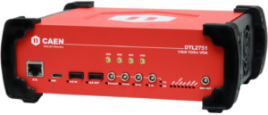
New DT2751 |
Desktop |
16 |
1000 |
500 |
[0.2 ÷ 2] |
14 |
84 M |
MCX |
DPP-PHA, DPP-PSD, D-SCOPE<sup>(cs)</sup> |
YES |
|
|
V1730 / V1730S |
VME |
8 / 16 |
500 |
250 |
0.5 - 2 |
14 |
640 k / 5.12 M |
MCX |
DPP-PHA, DPP-PSD, DPP-ZLEplus, D-WAVE |
NO |
|
|
N6725 / N6725S |
NIM |
8 |
250 |
125 |
0.5 - 2 |
14 |
640 k / 5.12 M |
MCX |
DPP-PHA, DPP-PSD, DPP-ZLEplus, DPP-DAW, D-WAVE |
NO |
|
|
New VX2751 |
VME64X |
16 |
1000 |
500 |
[0.2 ÷ 2] |
14 |
84 M |
MCX |
DPP-PHA, DPP-PSD, D-SCOPE<sup>(cs)</sup> |
YES |
|
|
VX1740 |
VME64X |
64 |
62.5 |
30 |
2 / 10 |
12 |
192 k / 1.5 M |
SMC 68P |
D-WAVE |
NO |
|
|
DT5740D |
Desktop |
32(SMC conn.) - 16(MCX conn) |
62.5 |
30 |
2 / 10 |
12 |
192 k |
SMC 68P - MCX |
DPP-QDC,D-WAVE |
NO |
|
|
V2745 |
VME |
64 |
125 |
20 |
[0.04 + 4] |
16 |
21 M |
2mm 40-pin header male |
DPP-PHA, DPP-PSD, D-SCOPE, DPP-ZLEplus<sup>(cs)</sup> |
YES |
|
|
DT5742 |
Desktop |
16 + 1 |
5000 (Based on DRS4 chip: 5 GS/s Switched Capacitor Array) |
500 |
1 |
12 |
0.128 / 1 |
MCX |
D-WAVE |
NO |
|
|
VX1725 / VX1725S |
VME64X |
8 / 16 |
250 |
125 |
0.5 - 2 |
14 |
640 k / 5.12 M |
MCX |
DPP-PHA, DPP-PSD, DPP-ZLEplus, DPP-DAW, D-WAVE |
NO |
|
|
VX1730 / VX1730S |
VME64X |
8 / 16 |
500 |
250 |
0.5 - 2 |
14 |
640 k / 5.12 M |
MCX |
DPP-PHA, DPP-PSD, DPP-ZLEplus, DPP-DAW, D-WAVE |
NO |
|
|
V2730B |
VME64 |
16 |
500 |
250 |
[0.2 ÷ 4] |
14 |
84 M |
MCX |
DPP-PHA, DPP-PSD, D-SCOPE(cs) |
YES |
|
|
N6730 / N6730S |
NIM |
8 |
500 |
250 |
0.5 - 2 |
14 |
640 k / 5.12 M |
MCX |
DPP-PHA, DPP-PSD, DPP-ZLEplus, DPP-DAW, D-WAVE |
NO |
|
|
V1743 |
VME |
16 |
3200 (Based on SAMLONG chip: 3.2 GS/s Switched Capacitor Array) |
500 |
2.5 |
12 |
0.007 M |
MCX |
D-WAVE |
NO |
|
|
VX1751 |
VME64X |
2(DES mode) - 4 |
2000(DES mode) - 1000 |
500 |
0.2 / 1 |
10 |
3.6 M(DES mode) - 1.8 M / 28.8 M(DES mode) - 14.4 M |
MCX |
DPP-PSD, DPP-ZLEplus, D-WAVE |
NO |
|

|
DT5740 |
Desktop |
32(SMC conn.) - 16(MCX conn) |
62.5 |
30 |
2 / 10 |
12 |
192 k |
SMC 68P - MCX |
D-WAVE |
NO |
|
|
V1720 |
VME |
8 |
250 |
125 |
2 |
12 |
1.25 M / 10 M |
MCX |
DPP-PSD, D-WAVE |
NO |
|
|
V1751 |
VME |
2(DES mode) - 4 |
2000(DES mode) - 1000 |
500 |
0.2 / 1 |
10 |
3.6 M(DES mode) - 1.8 M / 28.8 M(DES mode) - 14.4 M |
MCX |
DPP-PSD, DPP-ZLEplus, D-WAVE |
NO |
|
|
VX1742 |
VME64X |
32 + 2 |
5000 (Based on DRS4 chip: 5 GS/s Switched Capacitor Array) |
500 |
1 |
12 |
0.128 / 1 |
MCX |
D-WAVE |
NO |
|
|
DT5743 |
Desktop |
8 |
3200 (Based on SAMLONG chip: 3.2 GS/s Switched Capacitor Array) |
500 |
2.5 |
12 |
0.007 M |
MCX |
D-WAVE |
NO |
|
|
DT5720 |
Desktop |
4 / 2 |
250 |
125 |
2 |
12 |
1.25 M / 10 M |
MCX |
DPP-PSD, D-WAVE |
NO |
|
|
V1742 |
VME |
32 + 2 |
5000 (Based on DRS4 chip: 5 GS/s Switched Capacitor Array) |
500 |
1 |
12 |
0.128 / 1 |
MCX |
D-WAVE |
NO |
|
|
DT2730 |
Desktop |
32 / 16 |
500 |
250 |
[0.2 ÷ 4] |
14 |
84 M |
MCX |
DPP-PHA, DPP-PSD, D-SCOPE |
YES |
|
|
VX1743 |
VME64X |
16 |
3200 (Based on SAMLONG chip: 3.2 GS/s Switched Capacitor Array) |
500 |
2.5 |
12 |
0.007 M |
MCX |
D-WAVE |
NO |
|
|
V1740D |
VME |
64 |
62.5 |
30 |
2 / 10 |
12 |
192 k |
SMC 68P |
DPP-QDC, D-WAVE |
NO |
|
|
New DTL2751 |
Desktop |
4 |
1000 |
TBD |
TBD |
14 |
TBD |
MCX |
DPP-PSD(cs), D-SCOPE(cs) |
YES |
|
|
VX1720 |
VME64X |
8 |
250 |
125 |
2 |
12 |
1.25 M / 10 M |
MCX |
DPP-PSD, D-WAVE |
NO |
|
|
N6742 |
NIM |
16 + 1 |
5000 (Based on DRS4 chip: 5 GS/s Switched Capacitor Array) |
500 |
1 |
12 |
0.128 / 1 |
MCX |
D-WAVE |
NO |
Technical Specifications
|
GENERAL |
Form Factor: 1-unit wide VME64 Weight: 642 g Dimension: 6U x 160 mm |
||||
|
ANALOG INPUT |
|
||||
|
DIGITAL CONVERSION |
Resolution: 16 bits Sampling Rate: 125 MS/s simultaneously on each channel. Scalable by 2n decimation factor, n = 1 to 10 (Scope firmware only) |
||||
|
SYSTEM PERFORMANCE |
ENOB: 12 @ 5MHz, -3dB, Gain = 1 (Typ.) RMS: 3.6 LSB (≃ 110 µV) typical RMS @ Gain = 1 |
||||
|
DIGITAL I/O |
|
||||
|
DAC OUT |
|
||||
|
ACQUISITION MEMORY |
2.5 GB total DDR4 memory size (20.971 MS/ch) divisible in multiple buffers Maximum record length: ≃ 84 ms @ 125 MS/s (total memory size divided by 2)1 1 Value referred to the Scope firmware (minimum of two buffers admitted) |
||||
|
TRIGGER |
Modes
Trigger Time Stamp
|
||||
|
SYNCHRONIZATION |
|
||||
|
FIRMWARE |
Firmware stored in the on-board Flash Memory and live rebootable by Web Interface
|
||||
|
FPGA |
|
||||
|
OPEN FPGA |
|
||||
|
COMMUNICATION INTERFACES |
|
||||
|
SOFTWARE |
Readout SW – CoMPASS spectroscopy software (for DPP firmware only) – WaveDump2 (for Scope firmware only) SDK and Tools General purpose C libraries with demo samples for host Windows® and Linux® PC, and embedded Arm processor SCI-Compiler (Open FPGA) Automatic generation of drivers (USB, ethernet), libraries, and demo software for Windows®, Linux® Web Interface Firmware management (e,g. upgrades and on-the-fly selection of the firmware to run), board information, PLL and Ethernet configuration, board status monitoring |
||||
|
POWER REQUIREMENTS |
+12V: 1.4 A (Typ.) +5V: 9.0 A (Typ.) |
Footer