
Highlights
-
12 bit @ 5 GS/s, 1-unit wide NIM module
-
Switched Capacitor technology based on the DRS4 chip (designed at Paul Scherrer Institute)
-
1024 capacitor cells per channel (acquisition window of ~ 200 ns @ 5 GS/s)
-
-
5 GS/s, 2.5 GS/s, 1 GS/s, 750 MS/s software selectable sampling frequencies
-
16 analog input channels on MCX coaxial connectors
-
1 additional analog input (TR0):
-
fast (low latency) trigger
-
digitizable for high resolution timing (up to 50 ps)
-
-
1 Vpp input dynamic range (2 Vpp on request) with programmable DC offset adjustment
-
Dead-time due to conversion: 110 µs (analog inputs only), 181 µs (TR0 input)
-
Trigger modes:
-
External on TRG-IN connector; common to all groups
-
Fast (Low Latency) on TR0 connector; common to all groups
-
Self-trigger, combinations of channels over-threshold in logic OR; common to all groups
-
-
Memory buffer options: 128 events/ch; 1024 events/ch
-
USB and Optical Link communication interfaces
-
Demo software tools, C and LabVIEW libraries
Overview
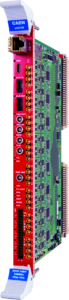
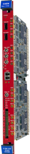
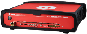
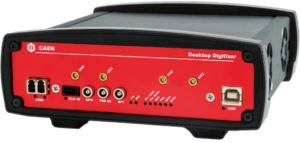
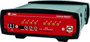
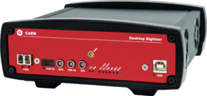
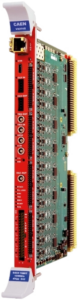
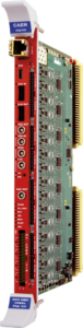
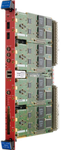
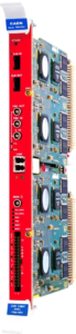
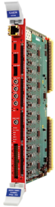
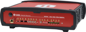
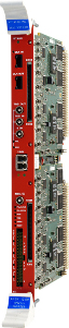
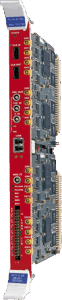
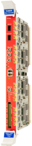
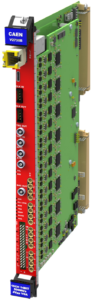
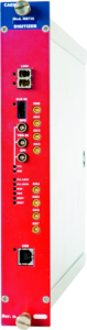
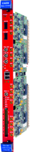
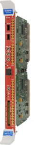
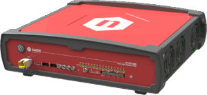
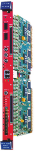
The CAEN Mod. N6742 is a NIM module housing 16+1 Channel 12 bit 5 GS/s Switched Capacitor Digitizer. The input dynamic range is 1 Vpp on single-ended MCX coaxial connectors (16-bit DAC on each channel to control the DC Offset).
The digitizer is based on the Switched Capacitor Array DRS4 chip (Domino Ring Sampler). This technology relies on a series of 1024 capacitors (analog memory) in which the analog input signal is continuously sampled in a circular way. The sampling frequency is 5 GHz by default and it can be programmed to 2.5 GHz, 1 GHz, and 750 MHz. The analog to digital conversion is not simultaneous with the chip sampling phase, and it starts as soon as the trigger condition is met, thus producing a dead time of 110 μs in case only the analog inputs are digitized, 181 μs when also the fast trigger TR0 is digitized. When the trigger stops the DRS4 chip sampling (holding phase), the analog memory buffer is frozen, and the cell content is made available to the 12 bit ADC for the digital conversion. The digital memory allows to store subsequent events, even if the readout is not yet started. Moreover, since the digital memory buffers work like FIFOs, the readout activity from USB or Optical Link does not affect write operations of subsequent events.
The available trigger sources are:
-
External Trigger, trigger on TRG-IN connector, common to all enabled groups.
-
Fast (Low Latency) Local Trigger, trigger on TR0 connector, common to all enabled groups. This mode is called “Fast” or “Low Latency” since the trigger latency to hold the DRS4 is reduced with respect to the external trigger. This trigger mode is convenient for high precision timing measurements, since the TR0 can be digitized and reported in the output data to be used as time reference.
-
Self-trigger, common to all enabled groups. For each group is possible to select combination of channels (logic OR) that provide a trigger whenever the input crosses the threshold. This mode cannot be used at 5 GHz due to the trigger latency.
The module features the front panel CLK IN connector and an internal PLL for clock synthesis from internal/external references. The module is available with digital memory sizes of 128 event/ch or 1024 event/ch.
N6742 houses USB 2.0 and Optical Link interfaces. USB 2.0 allows data transfers up to 30 MB/s. The Optical Link supports transfer rate of 80 MB/s and offers Daisy chain capability. Therefore, it is possible to connect up to 8/32 ADC modules to a single Optical Link Controller (Mod. A2818/A3818).
Software available (Windows and Linux):
CAEN provides drivers for all the different types of physical communication channels, a set of C and LabView libraries (CAENComm and CAENDigitizer), demo applications and utilities:
-
CAENUpgrader: tool that allows the user to update the firmware of the digitizers, change the PLL settings, load, when requested, the license for the pay firmware and other utilities.
Software for N6742 running Waveform Recording Firmware:
-
CAEN WaveDump: software console application that can be used to configure and readout event data from any model of the CAEN digitizer family and save the data into a memory buffer allocated for this purpose.
Software

CAEN Toolbox
CAENComm Library
Interface library for CAEN Data Acquistion Modules
CAENDigitizer Library
Library of functions for CAEN Digitizers high level management
WaveDump
Readout Application for CAEN Digitizer 1.0
WAVEDUMP2
Open Source Software for Digitizer 2.0 and 1.0 Series
Accessories
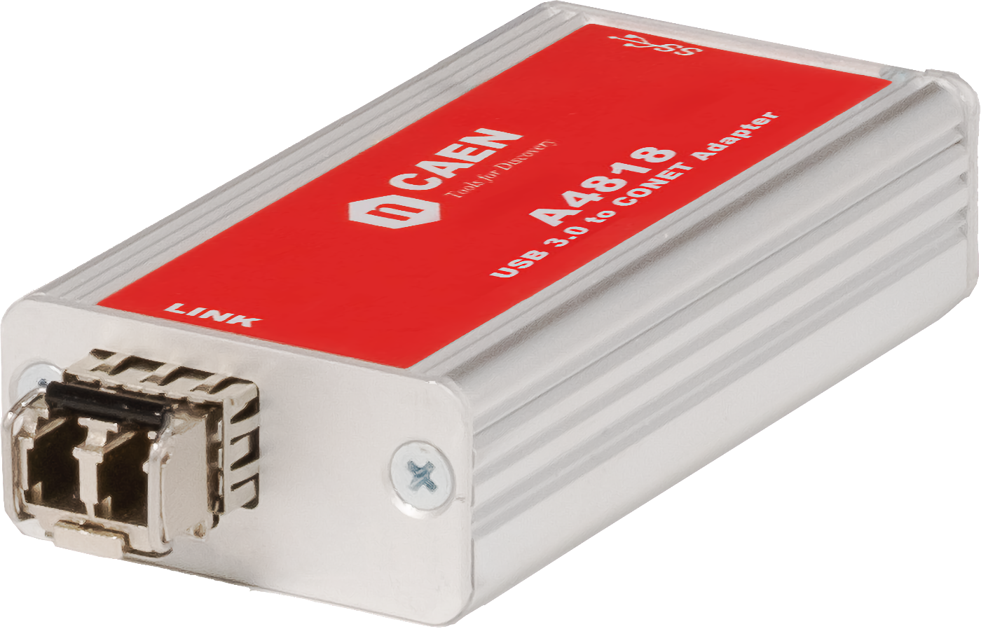
A4818

Digitizers Input Range Personalizations
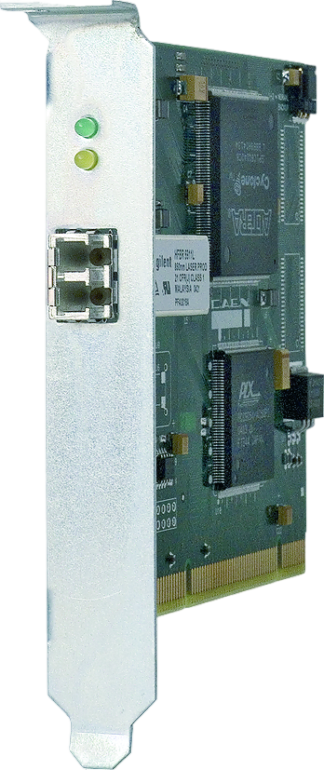
A2818
A318
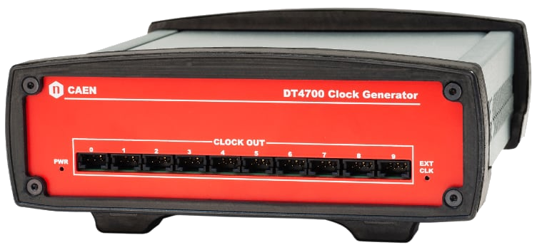
DT4700
A317
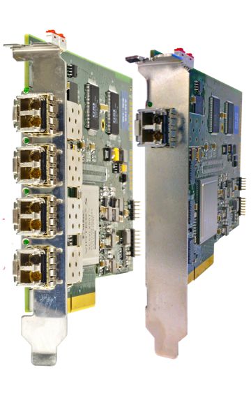
A3818
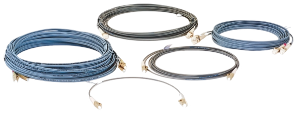
AI2700
A654
A659
You also may be interested in…
A4818
CAEN SyncTest x742
DT4700
NIM8302
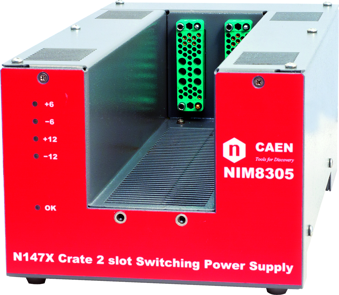
NIM8305
NV8020A
NIM8303
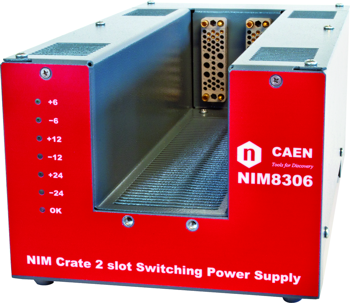
NIM8306
A5818
NIM8304
Request a Quote

Compare

|
Image
|
Name
|
Package
|
No. of Channels
|
Max Sampling Rate (MS/s)
|
Bandwidth (MHz)
|
Full Scale Range (V)
|
Resolution (bits)
|
Board Memory (Samples/ch)
|
Analog Input Connectors
|
CAEN firmware
|
Open FPGA
|
|
|
VX2730 |
VME64X |
32 |
500 |
250 |
[0.2 ÷ 4] |
14 |
84 M |
MCX |
DPP-PHA, DPP-PSD, D-SCOPE<sup>(cs)</sup> |
YES |
|
|
V1725 / V1725S |
VME |
8 / 16 |
250 |
125 |
0.5 - 2 |
14 |
640 k / 5.12 M |
MCX |
DPP-PHA, DPP-PSD, DPP-ZLEplus, D-WAVE |
NO |
|
|
DT2745 |
Desktop |
64 |
125 |
20 |
[0.04 + 4] |
16 |
21 M |
2mm 40-pin header male |
DPP-PHA, DPP-PSD, D-SCOPE, DPP-ZLEplus<sup>(cs)</sup> |
YES |
|
|
New R5560 |
rack mount 19 -2U |
128+6 |
125 |
60 |
2 |
14 |
max. 8k |
RJ45 |
n. a. |
YES |
|
|
New DTL2730 |
Desktop |
8 |
500 |
TBD |
TBD |
14 |
TBD |
MCX |
DPP-PHA(cs), DPP-PSD(cs), D-SCOPE(cs) |
YES |
|
|
V1761 |
VME |
2 |
4000 |
1000 |
1 |
10 |
7.2 M / 57.6 M |
MCX |
D-WAVE |
NO |
|
|
DT5751 |
Desktop |
2(DES mode) - 4 |
2000(DES mode) - 1000 |
500 |
0.2 / 1 |
10 |
3.6 M(DES mode) - 1.8 M |
MCX |
DPP-PSD, DPP-ZLEplus, D-WAVE |
NO |
|

|
VX1740D |
VME64X |
64 |
62.5 |
30 |
2 / 10 |
12 |
192 k |
SMC 68P |
DPP-QDC, D-WAVE |
NO |
|
|
DT5725 / DT5725S |
Desktop |
8 |
250 |
125 |
0.5 - 2 |
14 |
640 k / 5.12 M |
MCX |
DPP-PHA, DPP-PSD, DPP-ZLEplus, DPP-DAW, D-WAVE |
NO |
|
|
VX1724 |
VME64X |
8 |
100 |
40 |
0.5 / 2.25 / 10 |
14 |
512 k / 4 M |
MCX |
DPP-PHA, DPP-DAW |
NO |
|
|
DT5761 |
Desktop |
1 |
4000 |
1000 |
1 |
10 |
7.2 M |
MCX |
D-WAVE |
NO |
|
|
VX2745 |
VME64X |
64 |
125 |
20 |
[0.4 ÷ 4] |
16 |
21 M |
2mm 40-pin header male |
D-SCOPE, DPP-PHA, DPP-PSD, DPP-ZLEplus<sup>(cs)</sup> |
YES |
|
|
DT5724 |
Desktop |
4 / 2 |
100 |
40 |
0.5 / 2.25 / 10 |
14 |
512 k / 4 M |
MCX |
DPP-PHA, DPP-DAW, D-WAVE |
NO |
|
|
DT5730 / DT5730S |
Desktop |
8 |
500 |
250 |
0.5 - 2 |
14 |
640 k / 5.12 M |
MCX |
DPP-PHA, DPP-PSD, DPP-ZLEplus, DPP-DAW, D-WAVE |
NO |
|
|
VX2740 |
VME64X |
64 |
125 |
50 |
2 |
16 |
21 M |
2mm 40-pin header male |
DPP-PHA, D-SCOPE, DPP-PSD, DPP-ZLEplus<sup>(cs)</sup> |
YES |
|
|
V1724 |
VME |
8 |
100 |
40 |
0.5 / 2.25 / 10 |
14 |
512 k / 4 M |
MCX |
DPP-PHA, DPP-DAW, D-WAVE |
NO |
|
|
VX1761 |
VME64X |
2 |
4000 |
1000 |
1 |
10 |
7.2 M / 57.6 M |
MCX |
D-SCOPE |
NO |
|
|
DT2740 |
Desktop |
64 |
125 |
50 |
2 |
16 |
21 M |
2mm 40-pin header male |
DPP-PHA, DPP-PSD, D-SCOPE, DPP-ZLEplus<sup>(cs)</sup> |
YES |
|
|
V2740 |
VME |
64 |
125 |
50 |
2 |
16 |
21 M |
2mm 40-pin header male |
DPP-PHA, DPP-PSD, D-SCOPE, DPP-ZLEplus<sup>(cs)</sup> |
YES |
|
|
New DT2751 |
Desktop |
16 |
1000 |
500 |
[0.2 ÷ 2] |
14 |
84 M |
MCX |
DPP-PHA, DPP-PSD, D-SCOPE<sup>(cs)</sup> |
YES |
|
|
V1730 / V1730S |
VME |
8 / 16 |
500 |
250 |
0.5 - 2 |
14 |
640 k / 5.12 M |
MCX |
DPP-PHA, DPP-PSD, DPP-ZLEplus, D-WAVE |
NO |
|
|
N6725 / N6725S |
NIM |
8 |
250 |
125 |
0.5 - 2 |
14 |
640 k / 5.12 M |
MCX |
DPP-PHA, DPP-PSD, DPP-ZLEplus, DPP-DAW, D-WAVE |
NO |
|
|
New VX2751 |
VME64X |
16 |
1000 |
500 |
[0.2 ÷ 2] |
14 |
84 M |
MCX |
DPP-PHA, DPP-PSD, D-SCOPE<sup>(cs)</sup> |
YES |
|
|
VX1740 |
VME64X |
64 |
62.5 |
30 |
2 / 10 |
12 |
192 k / 1.5 M |
SMC 68P |
D-WAVE |
NO |
|
|
DT5740D |
Desktop |
32(SMC conn.) - 16(MCX conn) |
62.5 |
30 |
2 / 10 |
12 |
192 k |
SMC 68P - MCX |
DPP-QDC,D-WAVE |
NO |
|
|
V2745 |
VME |
64 |
125 |
20 |
[0.04 + 4] |
16 |
21 M |
2mm 40-pin header male |
DPP-PHA, DPP-PSD, D-SCOPE, DPP-ZLEplus<sup>(cs)</sup> |
YES |
|
|
DT5742 |
Desktop |
16 + 1 |
5000 (Based on DRS4 chip: 5 GS/s Switched Capacitor Array) |
500 |
1 |
12 |
0.128 / 1 |
MCX |
D-WAVE |
NO |
|
|
VX1725 / VX1725S |
VME64X |
8 / 16 |
250 |
125 |
0.5 - 2 |
14 |
640 k / 5.12 M |
MCX |
DPP-PHA, DPP-PSD, DPP-ZLEplus, DPP-DAW, D-WAVE |
NO |
|
|
VX1730 / VX1730S |
VME64X |
8 / 16 |
500 |
250 |
0.5 - 2 |
14 |
640 k / 5.12 M |
MCX |
DPP-PHA, DPP-PSD, DPP-ZLEplus, DPP-DAW, D-WAVE |
NO |
|
|
V2730B |
VME64 |
16 |
500 |
250 |
[0.2 ÷ 4] |
14 |
MCX |
84 M |
DPP-PHA, DPP-PSD, D-SCOPE(cs) |
YES |
|
|
N6730 / N6730S |
NIM |
8 |
500 |
250 |
0.5 - 2 |
14 |
640 k / 5.12 M |
MCX |
DPP-PHA, DPP-PSD, DPP-ZLEplus, DPP-DAW, D-WAVE |
NO |
|
|
V1743 |
VME |
16 |
3200 (Based on SAMLONG chip: 3.2 GS/s Switched Capacitor Array) |
500 |
2.5 |
12 |
0.007 M |
MCX |
D-WAVE |
NO |
|
|
VX1751 |
VME64X |
2(DES mode) - 4 |
2000(DES mode) - 1000 |
500 |
0.2 / 1 |
10 |
3.6 M(DES mode) - 1.8 M / 28.8 M(DES mode) - 14.4 M |
MCX |
DPP-PSD, DPP-ZLEplus, D-WAVE |
NO |
|

|
DT5740 |
Desktop |
32(SMC conn.) - 16(MCX conn) |
62.5 |
30 |
2 / 10 |
12 |
192 k |
SMC 68P - MCX |
D-WAVE |
NO |
|
|
V1720 |
VME |
8 |
250 |
125 |
2 |
12 |
1.25 M / 10 M |
MCX |
DPP-PSD, D-WAVE |
NO |
|
|
V1751 |
VME |
2(DES mode) - 4 |
2000(DES mode) - 1000 |
500 |
0.2 / 1 |
10 |
3.6 M(DES mode) - 1.8 M / 28.8 M(DES mode) - 14.4 M |
MCX |
DPP-PSD, DPP-ZLEplus, D-WAVE |
NO |
|
|
VX1742 |
VME64X |
32 + 2 |
5000 (Based on DRS4 chip: 5 GS/s Switched Capacitor Array) |
500 |
1 |
12 |
0.128 / 1 |
MCX |
D-WAVE |
NO |
|
|
DT5743 |
Desktop |
8 |
3200 (Based on SAMLONG chip: 3.2 GS/s Switched Capacitor Array) |
500 |
2.5 |
12 |
0.007 M |
MCX |
D-WAVE |
NO |
|
|
DT5720 |
Desktop |
4 / 2 |
250 |
125 |
2 |
12 |
1.25 M / 10 M |
MCX |
DPP-PSD, D-WAVE |
NO |
|
|
V1742 |
VME |
32 + 2 |
5000 (Based on DRS4 chip: 5 GS/s Switched Capacitor Array) |
500 |
1 |
12 |
0.128 / 1 |
MCX |
D-WAVE |
NO |
|
|
DT2730 |
Desktop |
32 / 16 |
500 |
250 |
[0.2 ÷ 4] |
14 |
MCX |
84 M |
DPP-PHA, DPP-PSD, D-SCOPE |
YES |
|
|
VX1743 |
VME64X |
16 |
3200 (Based on SAMLONG chip: 3.2 GS/s Switched Capacitor Array) |
500 |
2.5 |
12 |
0.007 M |
MCX |
D-WAVE |
NO |
|
|
V1740D |
VME |
64 |
62.5 |
30 |
2 / 10 |
12 |
192 k |
SMC 68P |
DPP-QDC, D-WAVE |
NO |
|
|
New DTL2751 |
Desktop |
4 |
1000 |
TBD |
TBD |
14 |
MCX |
TBD |
DPP-PSD(cs), D-SCOPE(cs) |
YES |
|
|
VX1720 |
VME64X |
8 |
250 |
125 |
2 |
12 |
1.25 M / 10 M |
MCX |
DPP-PSD, D-WAVE |
NO |
|
|
N6742 |
NIM |
16 + 1 |
5000 (Based on DRS4 chip: 5 GS/s Switched Capacitor Array) |
500 |
1 |
12 |
0.128 / 1 |
MCX |
D-WAVE |
NO |
Technical Specifications
|
GENERAL |
|
||||
|
ANALOG INPUT |
|
||||
|
DIGITAL CONVERSION |
|
||||
|
FPGA |
Altera Cyclone EP3C16 (one FPGA manages 16+1 channels) |
||||
|
TRIGGER |
|
||||
|
ACQUISITION MEMORY |
|
||||
|
ADC Clock generation |
|
||||
|
DIGITAL I/O |
|
||||
|
SYNCHRONIZATION |
|
||||
|
COMMUNICATION INTERFACES |
Optical Link: CAEN CONET proprietary protocol, Up to 80 MB/s transfer rate, Daisy‐chain capability |
||||
|
FIRMWARE |
Waveform Recording Firmware: Free firmware for waveform recording |
||||
|
SOFTWARE |
Readout SW: WaveDump readout software with C source files and VS project for developers (Windows® , Linux®) |
||||
|
ENVIRONMENTAL |
|
||||
|
Regulatory Compliance |
|
||||
|
POWER REQUIREMENTS |
|
Footer