
Highlights
-
12 bit 250 MS/s ADC
-
FPGA for real time Digital Pulse Processing:
-
8 input channels (single-ended)
-
2 Vpp input range
-
16-bit programmable DC offset adjustment: ±1 V independently on each channel
-
Trigger Time stamps
-
Multi-Event Memory buffer: 1.25 or 10 MS/ch, divisible into up to 1024 buffers
-
Programmable event size and pre-post trigger adjustment
-
Analog Sum/Majority and digital over/under threshold flags for Global Trigger logic
-
Front panel clock input/output available for multiboard synchronization (direct feed through or PLL-based synthesis)
-
16 programmable LVDS I/Os
-
Optical Link interface (CONET proprietary protocol) Daisy-chainable through A5818 (PCIe Gen 3) Controller or A4818 (USB3-to-CONET)
-
VME64X compliant interface
-
Firmware upgradeable via VME/Optical Link
Overview
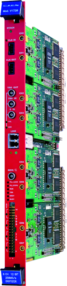
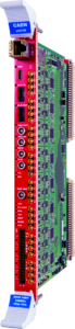
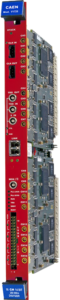
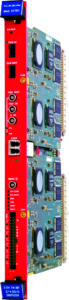
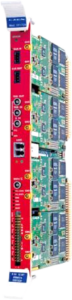
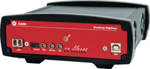
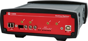
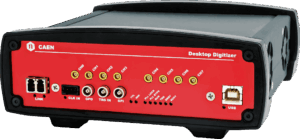
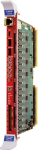
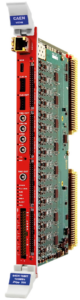
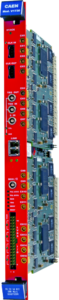
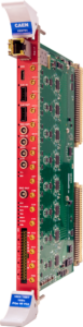
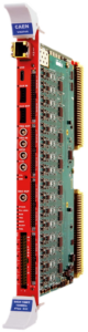
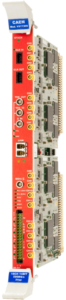
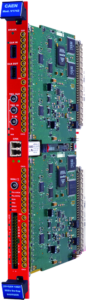
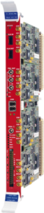
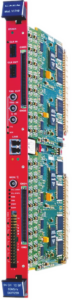
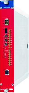
The CAEN Mod. V1720 is a Waveform Digitizer, housing 8 Input Channel 12 bit 250 MS/s Flash ADC, designed for waveform recording and supporting advanced algorithms for online digital pulse processing (DPP).
The individual DC offset adjustment (range ±1 V) by programmable 16bit DACs allows the effective sampling of either bipolar (Vin = ±1 V), or full positive (Vin = 0 ÷ +2 V), or negative (Vin = 0 ÷ -2 V) analog input swing without loosing dynamic resolution.
The module features front panel Clock Input and Output and mounts a PLL for the clock synthesis upon internal/external references. The data stream is continuously written in a circular memory buffer. When the trigger occurs, the FPGA writes further N samples for the post trigger and freezes the buffer that can be read either by VMEbus or Optical Link. The acquisition can continue without dead time in a new buffer.
Each channel has a SRAM Multi-Event Buffer divisible into 1 ÷ 1024 buffers of programmable size. Two sizes of the channel digital memory are available by ordering options: 1.25 MS/ch (mod. V1720E) and 10 MS/ch (mod. V1720G). “Zero suppression” and “data reduction” algorithms allow substantial savings in data amount readout and processing, rejecting samples smaller than a programmable threshold. The V1720 supports multi-board synchronization allowing all ADCs to be synchronized to a common clock source and ensuring Trigger time stamp and Data alignment.
The trigger for the event acquisition can be provided either externally via the front panel Trigger Input, or by software command, or it is internally generated upon the self-trigger capability (i.e. individual discriminator on each channel with programmable threshold). The trigger from one board can be propagated to the other boards through the front panel Trigger Output.
An Analog Output is available with four operating modes supported:
-
Waveform Generator: 1 Vpp test ramp
-
Majority: output signal is proportional to the number of input channels under/over threshold (1 step = 125 mV)
-
Buffer Occupancy: output signal is proportional to the Multi Event Buffer Occupancy: 1 buffer ~ 1 mV
-
Voltage level: output signal is a programmable voltage level (0 to +1 V range with 12-bit resolution)
The V1720 houses VME (VME64X compliant) and Optical Link interfaces. The VME interface allows data transfers of 60 MB/s (MBLT64), 100 MB/s (2eVME), 160 MB/s (2eSST). The Optical Link supports transfer rate of 80 MB/s and offers Daisy chain capability. Therefore, it is possible to connect up to 8 ADC modules to the single-link A4818 Adapter, while up to 32 ADC modules to the 4-link A5818 .
Software available (Windows and Linux):
CAEN provides drivers for all the different types of physical communication channels, a set of C, Python, and LabView libraries (CAENComm and CAENDigitizer), demo applications and utilities:
-
CAEN Toolbox: tool that allows the user to update the firmware of the digitizers, change the PLL settings, load, when requested, the license for the pay firmware and other utilities.
-
CAEN WaveDump: C-based readout program for the single-board management or Digitizer 1.0 Series running the Waveform Recording firmware, provided with source files for user customization.
-
WaveDump2: Open source GUI-based application for the single and multi-board management of Digitizer 2.0 and 1.0 Series running the Waveform Recording / Scope firmware.
-
CoMPASS: Multiparametric DAQ Software for Physics Applications with single and multi-board support of Digitizer 2.0 and 1.0 Series running the DPP firmware.
CAEN provides also for this model Digital Pulse Processing firmware for Physics Applications. This feature allows to perform on-line processing on detector signal directly digitized:
-
DPP-PSD Digital Pulse Processing for Pulse Shape Discrimination
x720(*) and x751 digitizers running DPP-PSD firmware accept signals directly from the detector and implement a digital replacement of dual gate QDC, discriminator and gate generator.
(*) DPP-CI firmware and DPP-CI Control Software are no longer supported. To perform Charge Integration please refer to the DPP-PSD firmware and software.
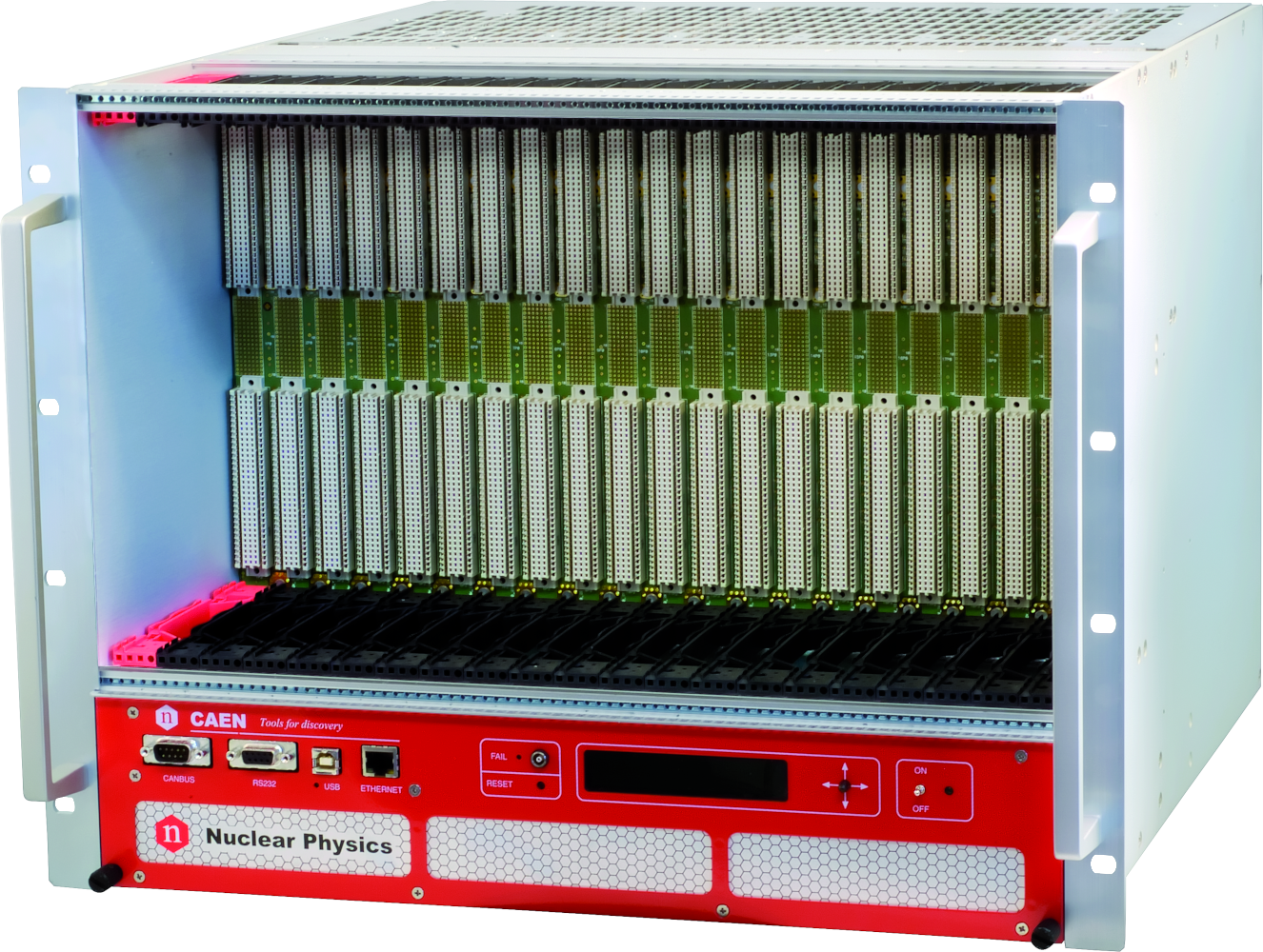
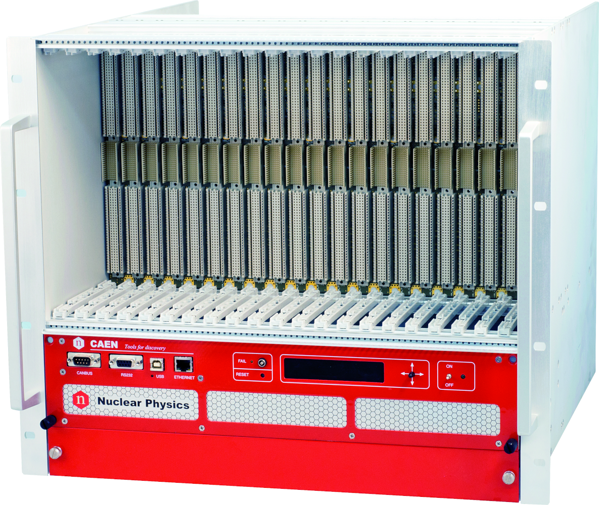
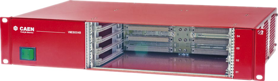
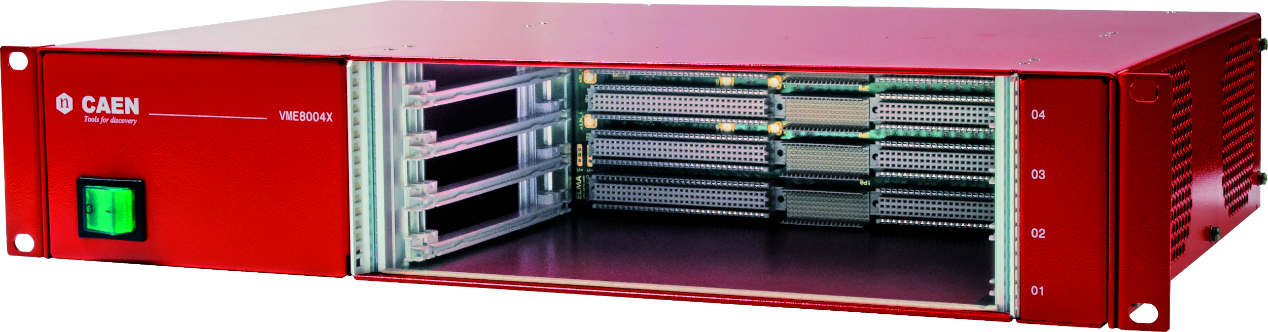
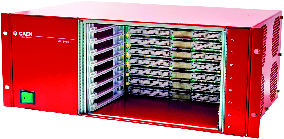
Note: V1720 can be operated with VME8004B / VME8004X / VME8008B / VME8008X /NV8020A/VME8010 / VME8011 / VME8100 / VME8200/μ-crate.
Never use this digitizer with crates VME8001, VME8002, VME8004, and VME8004A. Overheat may damage the module.
Software

CAEN Toolbox
CAENComm Library
Interface library for CAEN Data Acquistion Modules
CAENDigitizer Library
Library of functions for CAEN Digitizers high level management

COMPASS
WaveDump
Readout Application for CAEN Digitizer 1.0

CAEN FELib Library
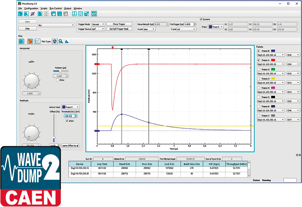
WAVEDUMP2
Open Source Software for Digitizer 2.0 and 1.0 Series

Accessories
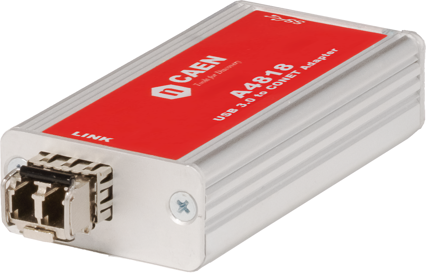
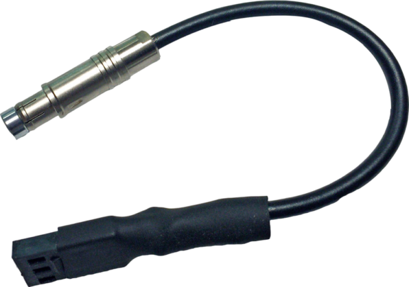
A4818
A954
A316
A318
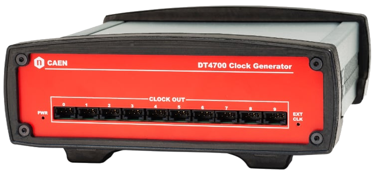
DT4700
A317
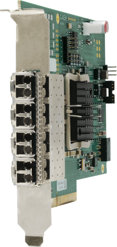
A5818
CONET2 Controller based on PCI Express Gen 3 interface
A319B
AI2700
A654
A659
A952
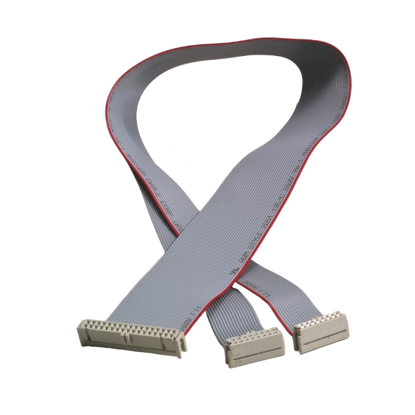
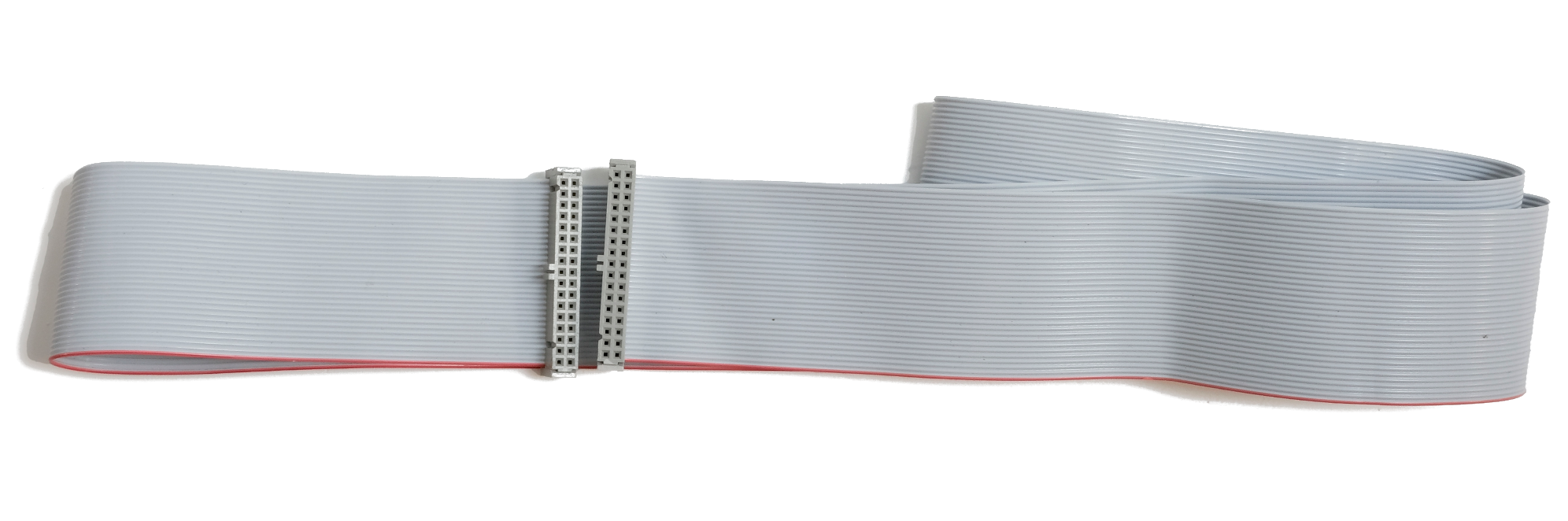
Cable assembly 2.54mm 34 pin female to 2.54mm 34 pin female - 50 cm
A953
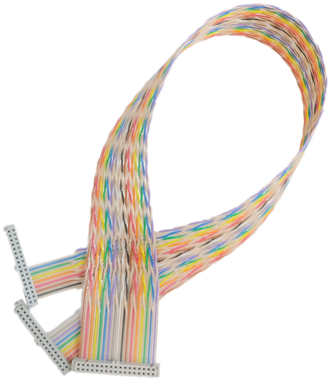
Cable assembly 2.54mm 34 pin female to two 2.54mm 34 pin female – 50 cm
You also may be interested in…
A4818
DT5720
VME8008B
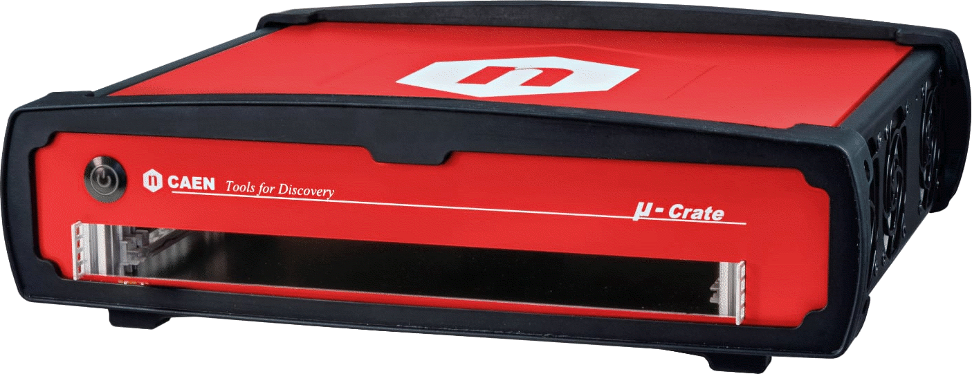
µ-crate
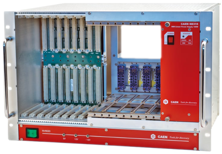
NV8020A
VME8100
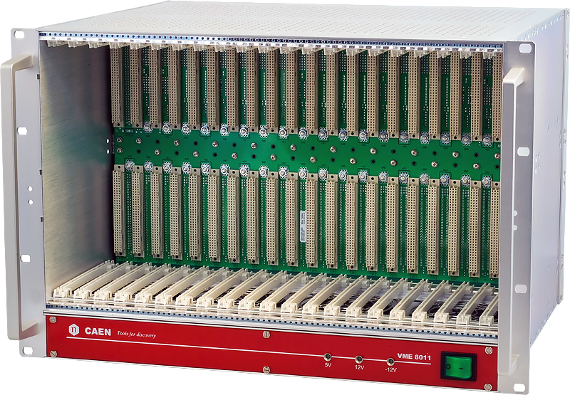
VME8011
VME8200
VX1720
A5818
V3718
V4718
VME8004B
VME8004X
VME8008X
Request a Quote

Compare

|
Image
|
Name
|
Package
|
No. of Channels
|
Max Sampling Rate (MS/s)
|
Bandwidth (MHz)
|
Full Scale Range (V)
|
Resolution (bits)
|
Board Memory (Samples/ch)
|
Analog Input Connectors
|
CAEN firmware
|
Open FPGA
|
|
|
VX2730 |
VME64X |
32 |
500 |
250 |
[0.2 ÷ 4] |
14 |
84 M |
MCX |
DPP-PHA, DPP-PSD, D-SCOPE<sup>(cs)</sup> |
YES |
|
|
V1725 / V1725S |
VME |
8 / 16 |
250 |
125 |
0.5 - 2 |
14 |
640 k / 5.12 M |
MCX |
DPP-PHA, DPP-PSD, DPP-ZLEplus, D-WAVE |
NO |
|
|
DT2745 |
Desktop |
64 |
125 |
20 |
[0.04 + 4] |
16 |
21 M |
2mm 40-pin header male |
DPP-PHA, DPP-PSD, D-SCOPE, DPP-ZLEplus<sup>(cs)</sup> |
YES |
|
|
New R5560 |
rack mount 19 -2U |
128+6 |
125 |
60 |
2 |
14 |
max. 8k |
RJ45 |
n. a. |
YES |
|
|
New DTL2730 |
Desktop |
8 |
500 |
TBD |
TBD |
14 |
TBD |
MCX |
DPP-PHA(cs), DPP-PSD(cs), D-SCOPE(cs) |
YES |
|
|
V1761 |
VME |
2 |
4000 |
1000 |
1 |
10 |
7.2 M / 57.6 M |
MCX |
D-WAVE |
NO |
|
|
DT5751 |
Desktop |
2(DES mode) - 4 |
2000(DES mode) - 1000 |
500 |
0.2 / 1 |
10 |
3.6 M(DES mode) - 1.8 M |
MCX |
DPP-PSD, DPP-ZLEplus, D-WAVE |
NO |
|

|
VX1740D |
VME64X |
64 |
62.5 |
30 |
2 / 10 |
12 |
192 k |
SMC 68P |
DPP-QDC, D-WAVE |
NO |
|
|
DT5725 / DT5725S |
Desktop |
8 |
250 |
125 |
0.5 - 2 |
14 |
640 k / 5.12 M |
MCX |
DPP-PHA, DPP-PSD, DPP-ZLEplus, DPP-DAW, D-WAVE |
NO |
|
|
VX1724 |
VME64X |
8 |
100 |
40 |
0.5 / 2.25 / 10 |
14 |
512 k / 4 M |
MCX |
DPP-PHA, DPP-DAW |
NO |
|
|
DT5761 |
Desktop |
1 |
4000 |
1000 |
1 |
10 |
7.2 M |
MCX |
D-WAVE |
NO |
|
|
VX2745 |
VME64X |
64 |
125 |
20 |
[0.4 ÷ 4] |
16 |
21 M |
2mm 40-pin header male |
D-SCOPE, DPP-PHA, DPP-PSD, DPP-ZLEplus<sup>(cs)</sup> |
YES |
|
|
DT5724 |
Desktop |
4 / 2 |
100 |
40 |
0.5 / 2.25 / 10 |
14 |
512 k / 4 M |
MCX |
DPP-PHA, DPP-DAW, D-WAVE |
NO |
|
|
DT5730 / DT5730S |
Desktop |
8 |
500 |
250 |
0.5 - 2 |
14 |
640 k / 5.12 M |
MCX |
DPP-PHA, DPP-PSD, DPP-ZLEplus, DPP-DAW, D-WAVE |
NO |
|
|
VX2740 |
VME64X |
64 |
125 |
50 |
2 |
16 |
21 M |
2mm 40-pin header male |
DPP-PHA, D-SCOPE, DPP-PSD, DPP-ZLEplus<sup>(cs)</sup> |
YES |
|
|
V1724 |
VME |
8 |
100 |
40 |
0.5 / 2.25 / 10 |
14 |
512 k / 4 M |
MCX |
DPP-PHA, DPP-DAW, D-WAVE |
NO |
|
|
VX1761 |
VME64X |
2 |
4000 |
1000 |
1 |
10 |
7.2 M / 57.6 M |
MCX |
D-SCOPE |
NO |
|
|
DT2740 |
Desktop |
64 |
125 |
50 |
2 |
16 |
21 M |
2mm 40-pin header male |
DPP-PHA, DPP-PSD, D-SCOPE, DPP-ZLEplus<sup>(cs)</sup> |
YES |
|
|
V2740 |
VME |
64 |
125 |
50 |
2 |
16 |
21 M |
2mm 40-pin header male |
DPP-PHA, DPP-PSD, D-SCOPE, DPP-ZLEplus<sup>(cs)</sup> |
YES |
|
|
New DT2751 |
Desktop |
16 |
1000 |
500 |
[0.2 ÷ 2] |
14 |
84 M |
MCX |
DPP-PHA, DPP-PSD, D-SCOPE<sup>(cs)</sup> |
YES |
|
|
V1730 / V1730S |
VME |
8 / 16 |
500 |
250 |
0.5 - 2 |
14 |
640 k / 5.12 M |
MCX |
DPP-PHA, DPP-PSD, DPP-ZLEplus, D-WAVE |
NO |
|
|
N6725 / N6725S |
NIM |
8 |
250 |
125 |
0.5 - 2 |
14 |
640 k / 5.12 M |
MCX |
DPP-PHA, DPP-PSD, DPP-ZLEplus, DPP-DAW, D-WAVE |
NO |
|
|
New VX2751 |
VME64X |
16 |
1000 |
500 |
[0.2 ÷ 2] |
14 |
84 M |
MCX |
DPP-PHA, DPP-PSD, D-SCOPE<sup>(cs)</sup> |
YES |
|
|
VX1740 |
VME64X |
64 |
62.5 |
30 |
2 / 10 |
12 |
192 k / 1.5 M |
SMC 68P |
D-WAVE |
NO |
|
|
DT5740D |
Desktop |
32(SMC conn.) - 16(MCX conn) |
62.5 |
30 |
2 / 10 |
12 |
192 k |
SMC 68P - MCX |
DPP-QDC,D-WAVE |
NO |
|
|
V2745 |
VME |
64 |
125 |
20 |
[0.04 + 4] |
16 |
21 M |
2mm 40-pin header male |
DPP-PHA, DPP-PSD, D-SCOPE, DPP-ZLEplus<sup>(cs)</sup> |
YES |
|
|
DT5742 |
Desktop |
16 + 1 |
5000 (Based on DRS4 chip: 5 GS/s Switched Capacitor Array) |
500 |
1 |
12 |
0.128 / 1 |
MCX |
D-WAVE |
NO |
|
|
VX1725 / VX1725S |
VME64X |
8 / 16 |
250 |
125 |
0.5 - 2 |
14 |
640 k / 5.12 M |
MCX |
DPP-PHA, DPP-PSD, DPP-ZLEplus, DPP-DAW, D-WAVE |
NO |
|
|
VX1730 / VX1730S |
VME64X |
8 / 16 |
500 |
250 |
0.5 - 2 |
14 |
640 k / 5.12 M |
MCX |
DPP-PHA, DPP-PSD, DPP-ZLEplus, DPP-DAW, D-WAVE |
NO |
|
|
V2730B |
VME64 |
16 |
500 |
250 |
[0.2 ÷ 4] |
14 |
MCX |
84 M |
DPP-PHA, DPP-PSD, D-SCOPE(cs) |
YES |
|
|
N6730 / N6730S |
NIM |
8 |
500 |
250 |
0.5 - 2 |
14 |
640 k / 5.12 M |
MCX |
DPP-PHA, DPP-PSD, DPP-ZLEplus, DPP-DAW, D-WAVE |
NO |
|
|
V1743 |
VME |
16 |
3200 (Based on SAMLONG chip: 3.2 GS/s Switched Capacitor Array) |
500 |
2.5 |
12 |
0.007 M |
MCX |
D-WAVE |
NO |
|
|
VX1751 |
VME64X |
2(DES mode) - 4 |
2000(DES mode) - 1000 |
500 |
0.2 / 1 |
10 |
3.6 M(DES mode) - 1.8 M / 28.8 M(DES mode) - 14.4 M |
MCX |
DPP-PSD, DPP-ZLEplus, D-WAVE |
NO |
|

|
DT5740 |
Desktop |
32(SMC conn.) - 16(MCX conn) |
62.5 |
30 |
2 / 10 |
12 |
192 k |
SMC 68P - MCX |
D-WAVE |
NO |
|
|
V1720 |
VME |
8 |
250 |
125 |
2 |
12 |
1.25 M / 10 M |
MCX |
DPP-PSD, D-WAVE |
NO |
|
|
V1751 |
VME |
2(DES mode) - 4 |
2000(DES mode) - 1000 |
500 |
0.2 / 1 |
10 |
3.6 M(DES mode) - 1.8 M / 28.8 M(DES mode) - 14.4 M |
MCX |
DPP-PSD, DPP-ZLEplus, D-WAVE |
NO |
|
|
VX1742 |
VME64X |
32 + 2 |
5000 (Based on DRS4 chip: 5 GS/s Switched Capacitor Array) |
500 |
1 |
12 |
0.128 / 1 |
MCX |
D-WAVE |
NO |
|
|
DT5743 |
Desktop |
8 |
3200 (Based on SAMLONG chip: 3.2 GS/s Switched Capacitor Array) |
500 |
2.5 |
12 |
0.007 M |
MCX |
D-WAVE |
NO |
|
|
DT5720 |
Desktop |
4 / 2 |
250 |
125 |
2 |
12 |
1.25 M / 10 M |
MCX |
DPP-PSD, D-WAVE |
NO |
|
|
V1742 |
VME |
32 + 2 |
5000 (Based on DRS4 chip: 5 GS/s Switched Capacitor Array) |
500 |
1 |
12 |
0.128 / 1 |
MCX |
D-WAVE |
NO |
|
|
DT2730 |
Desktop |
32 / 16 |
500 |
250 |
[0.2 ÷ 4] |
14 |
MCX |
84 M |
DPP-PHA, DPP-PSD, D-SCOPE |
YES |
|
|
VX1743 |
VME64X |
16 |
3200 (Based on SAMLONG chip: 3.2 GS/s Switched Capacitor Array) |
500 |
2.5 |
12 |
0.007 M |
MCX |
D-WAVE |
NO |
|
|
V1740D |
VME |
64 |
62.5 |
30 |
2 / 10 |
12 |
192 k |
SMC 68P |
DPP-QDC, D-WAVE |
NO |
|
|
New DTL2751 |
Desktop |
4 |
1000 |
TBD |
TBD |
14 |
MCX |
TBD |
DPP-PSD(cs), D-SCOPE(cs) |
YES |
|
|
VX1720 |
VME64X |
8 |
250 |
125 |
2 |
12 |
1.25 M / 10 M |
MCX |
DPP-PSD, D-WAVE |
NO |
|
|
N6742 |
NIM |
16 + 1 |
5000 (Based on DRS4 chip: 5 GS/s Switched Capacitor Array) |
500 |
1 |
12 |
0.128 / 1 |
MCX |
D-WAVE |
NO |
Technical Specifications
|
GENERAL |
|
|||||||||
|
ANALOG INPUT |
|
|||||||||
|
DIGITAL CONVERSION |
*The minimum value may depend on the digitizer model, the firmware, and the hardware downsampling mode. |
|||||||||
|
SYSTEM PERFORMANCE |
|
|||||||||
|
DIGITAL I/O |
|
|||||||||
|
ANALOG OUT |
|
|||||||||
|
ACQUISITION MEMORY |
|
|||||||||
|
COMMUNICATION INTERFACES |
|
|||||||||
|
TRIGGER AND EVENT ACQUISITION |
|
|||||||||
|
SYNCHRONIZATION |
|
|||||||||
|
FPGA |
|
|||||||||
|
CAEN FIRMWARE |
Developed by CAEN, stored in the on-board FLASH memory.
|
|||||||||
|
SOFTWARE |
|
|||||||||
|
ENVIRONMENTAL |
|
|||||||||
|
REGULATORY COMPLIANCE |
|
|||||||||
|
POWER CONSUMPTIONS |
+5 V: 4.0 A (Typ.) |
Footer