
Highlights
-
14 bit 100 MS/s ADC
-
FPGA for real time Digital Pulse Processing:
-
8 input channels (single-ended)
-
2.25 Vpp input range (default); 10 Vpp and 0.5 Vpp customization by ordering option
-
16-bit programmable DC offset adjustment in the full range independently on each channel
-
Sampling rate decimation factor
-
Trigger Time stamps
-
Multi-Event Memory buffer: 512 kS/ch or 4 MS/ch, divisible into up to 1024 buffers
-
Programmable event size and pre-post trigger adjustment
-
Signal Inspection/Analog Sum/Majority and digital over/under threshold flags for Global Trigger logic
-
Front panel clock input/output available for multiboard synchronization (direct feed through or PLL-based synthesis)
-
16 programmable LVDS I/Os
-
Optical Link interface (CONET proprietary protocol) Daisy-chainable through A5818 (PCIe Gen 3) Controller or A4818 (USB3-to-CONET)
-
VME64X compliant interface
-
Firmware upgradeable via VME/Optical Link
Overview
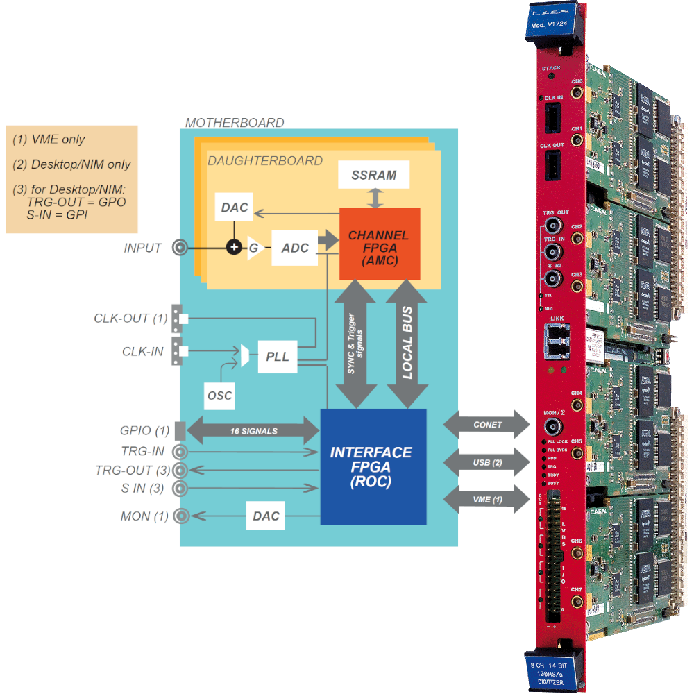
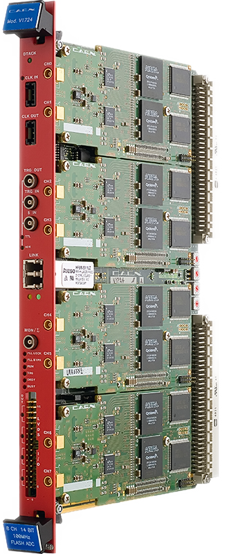
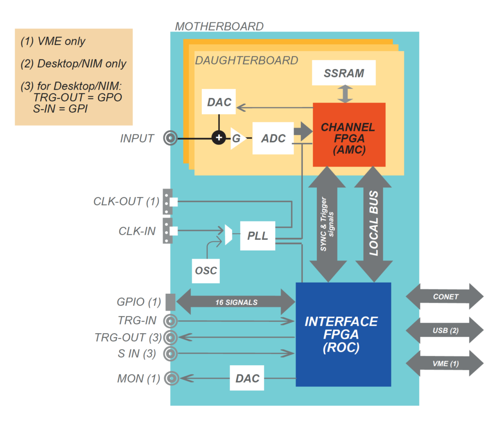
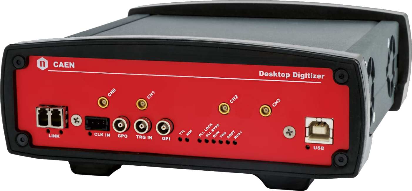
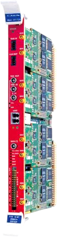
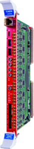
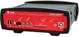
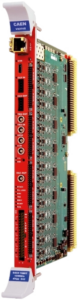
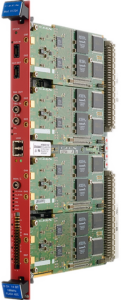
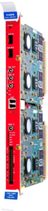
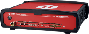
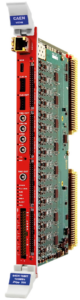
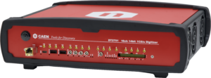
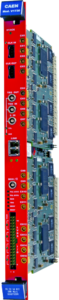
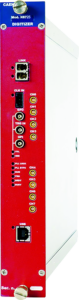
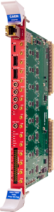
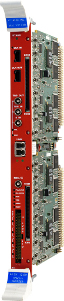
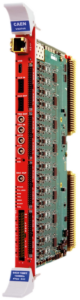
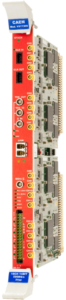
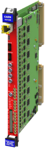
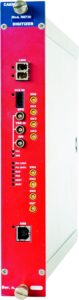
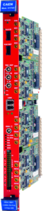
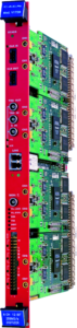
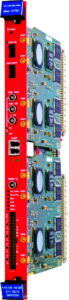
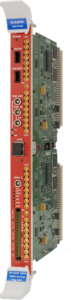
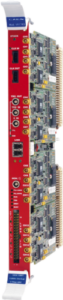
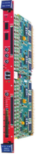
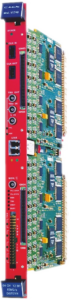
The CAEN Mod. V1724 is a Waveform Digitizer, in VME64 form factor, housing 8 Input Channel 14 bit 100 MS/s Flash ADC, designed for waveform recording and supporting advanced algorithms for online digital pulse processing (DPP).
The Digitizer is well suited for high-resolution detectors as Silicon, HPGe or inorganic scintillators like NaI or CsI coupled with Charge Sensitive Preamplifiers. In the waveform recording mode, algorithms of zero suppression are also implemented to reduce the data throughput. The acquisition can be channel independent and it is possible to make coincidence/anti-coincidence logic among different channels and external veto/gating. Multiple boards can be synchronized to build up complex systems.
In the case of DPP mode, data can be saved in time-stamped list mode to support higher input rates and improve the throughput performances. Piled-up events can be rejected or saved for offline analysis. The acquisition in DPP-PHA mode is fully controlled by the CoMPASS software, which manages the algorithm parameters, build the plots and saves the relevant energy and time spectra. In the case of waveform recording mode, the user can take advantage of the WaveDump or WaveDump2 software to access and save the waveforms. For DPP-DAW mode, a C demo fully controls the acquisition, data plotting and saving.
Libraries and demo software in C, Phyton, and LabView are available for integration and customization of specific acquisition systems.
The communication to and from the board is provided through the VMEBus and Optical Link interfaces.
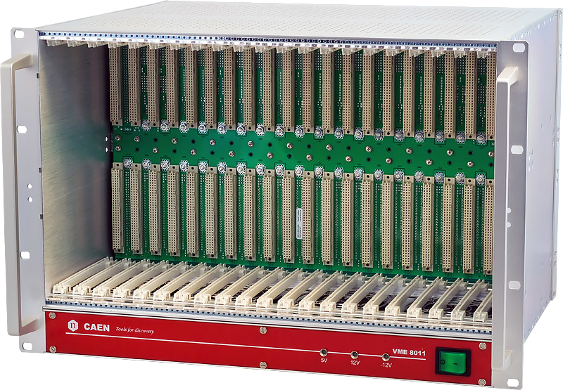
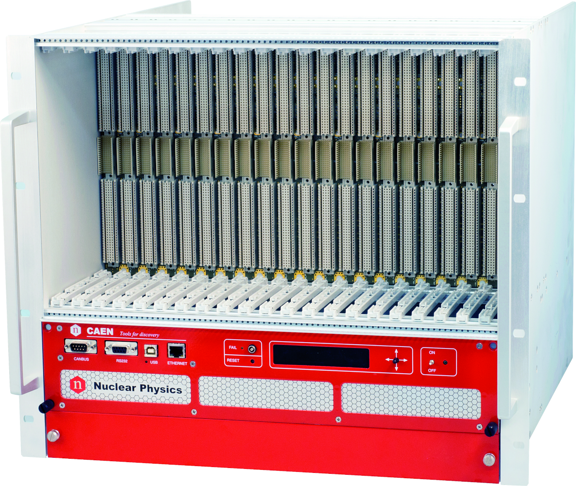
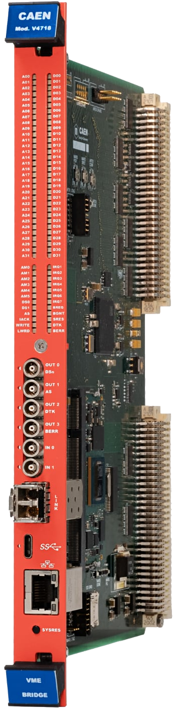
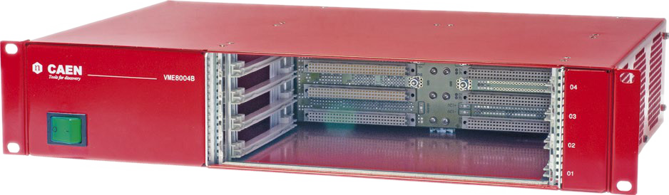
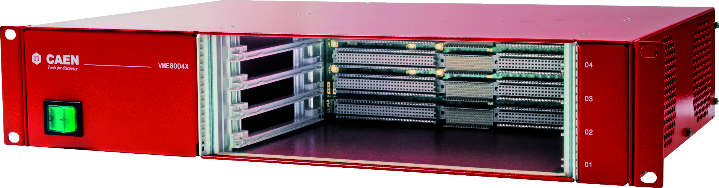
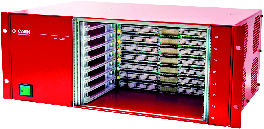
Note: V1724 can be operated with VME8004B / VME8004X / VME8008B / VME8008X /NV8020A/VME8010 / VME8011 / VME8100 / VME8200/μ-crate.
Never use this digitizer with crates VME8001, VME8002, VME8004, and VME8004A. Overheat may damage the module.
Software

CAEN Toolbox

CAENComm Library
Interface library for CAEN Data Acquistion Modules
CAENDigitizer Library
Library of functions for CAEN Digitizers high level management
CAENDPP Library
High level library for CAEN Digitizers running DPP firmware

COMPASS
WaveDump
Readout Application for CAEN Digitizer 1.0

CAEN FELib Library
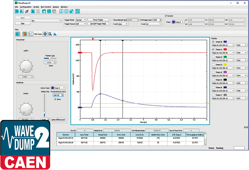
WAVEDUMP2
Open Source Software for Digitizer 2.0 and 1.0 Series

Accessories
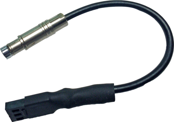
A4818
A954

Digitizers Input Range Personalizations
A316
A318
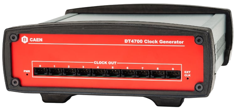
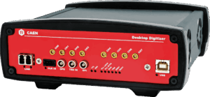
DT4700
A317
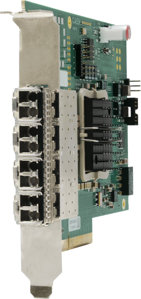
A5818
CONET2 Controller based on PCI Express Gen 3 interface
A319B
AI2700
A654
A659
A952
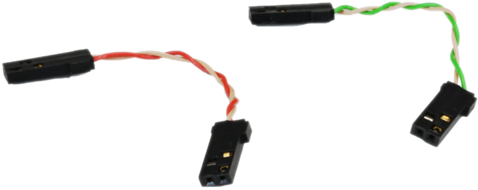
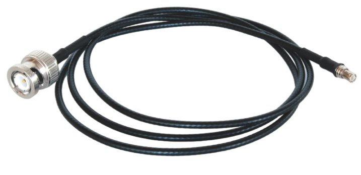
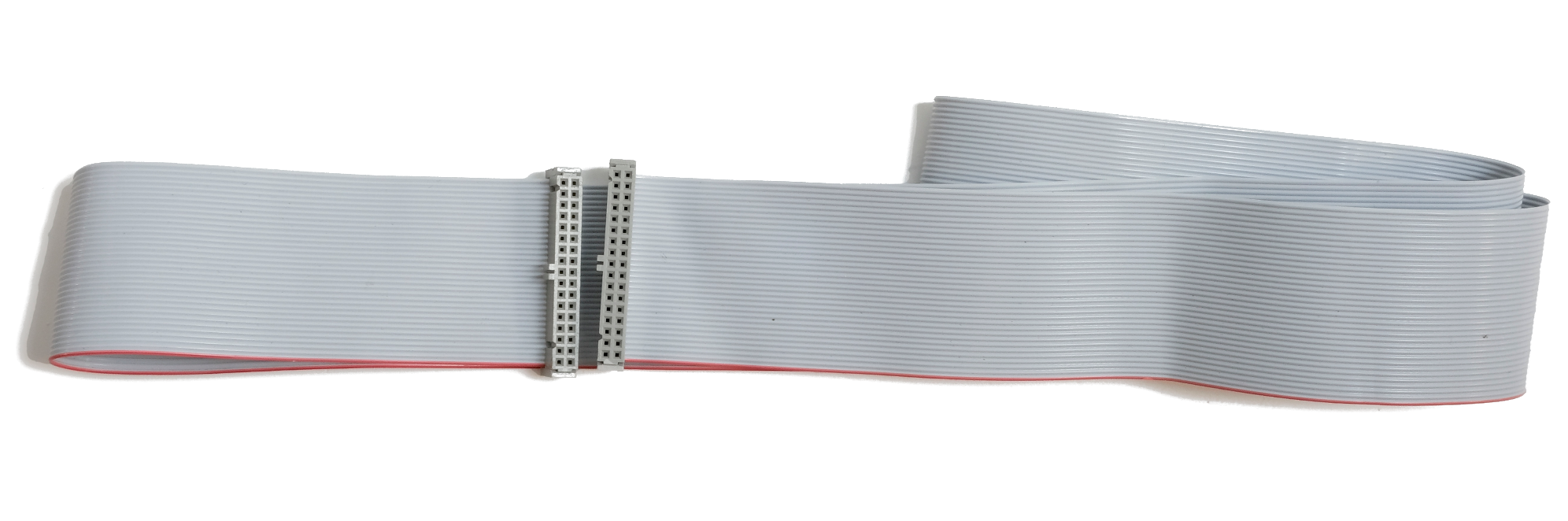
Cable assembly 2.54mm 34 pin female to 2.54mm 34 pin female - 50 cm
A953
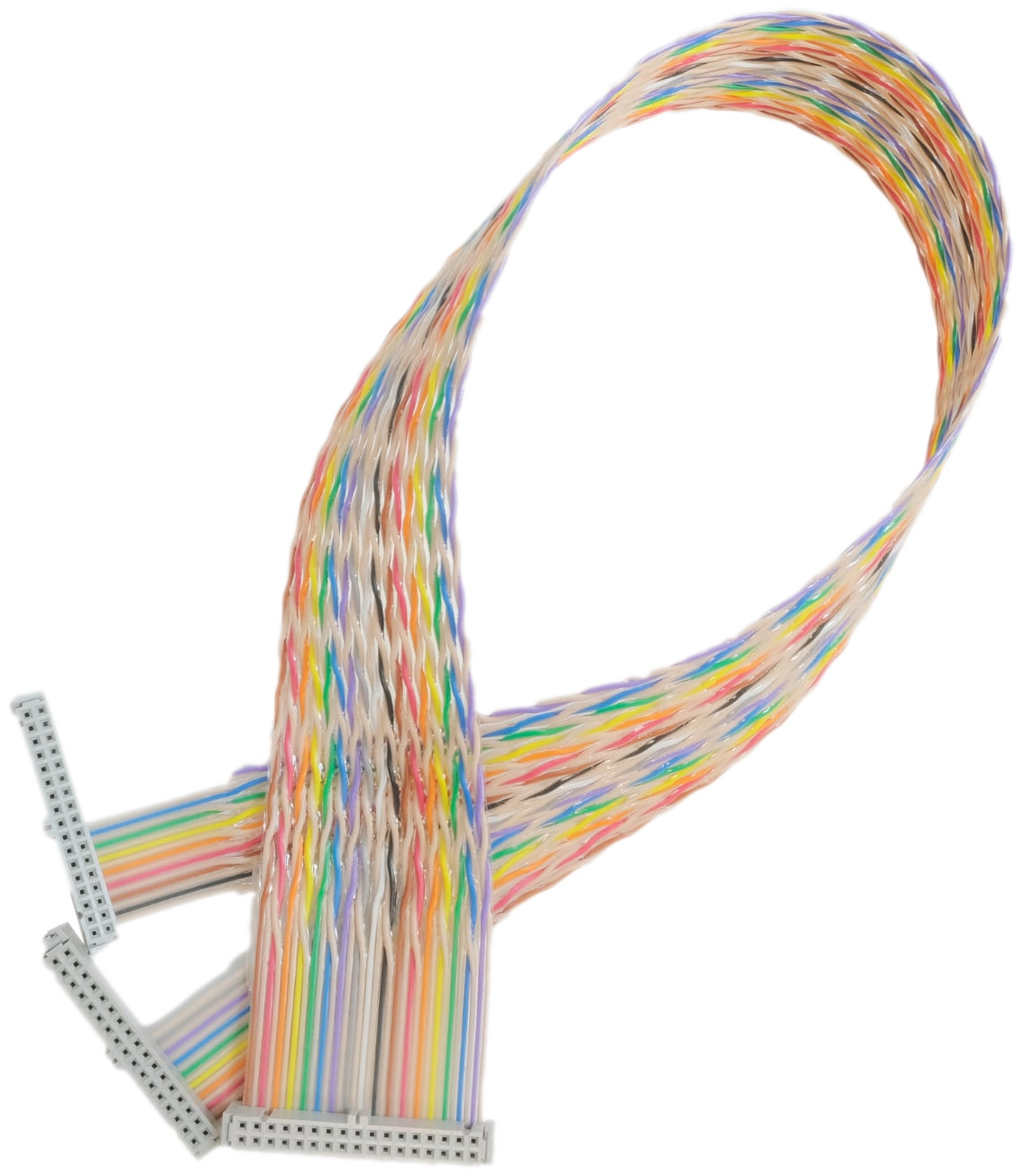
Cable assembly 2.54mm 34 pin female to two 2.54mm 34 pin female – 50 cm
You also may be interested in…
A4818
DT5724
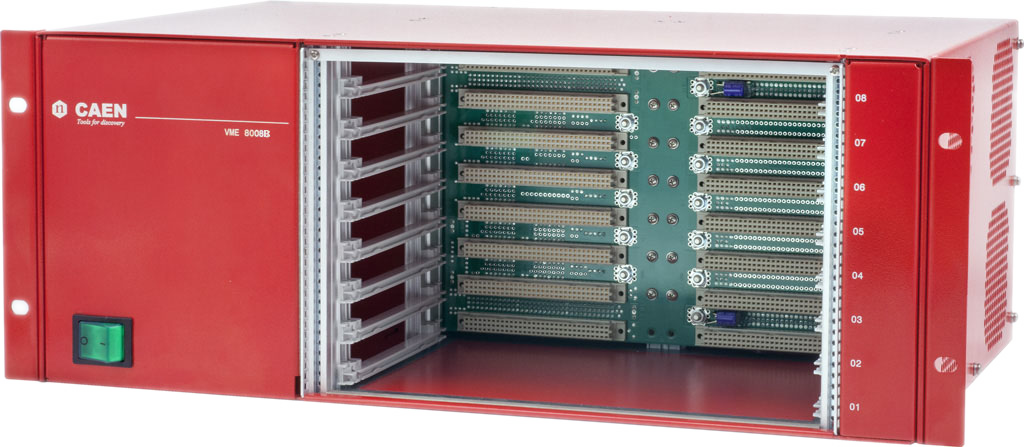
VME8008B
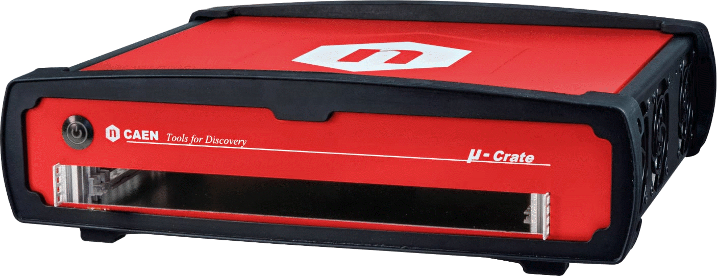
µ-crate
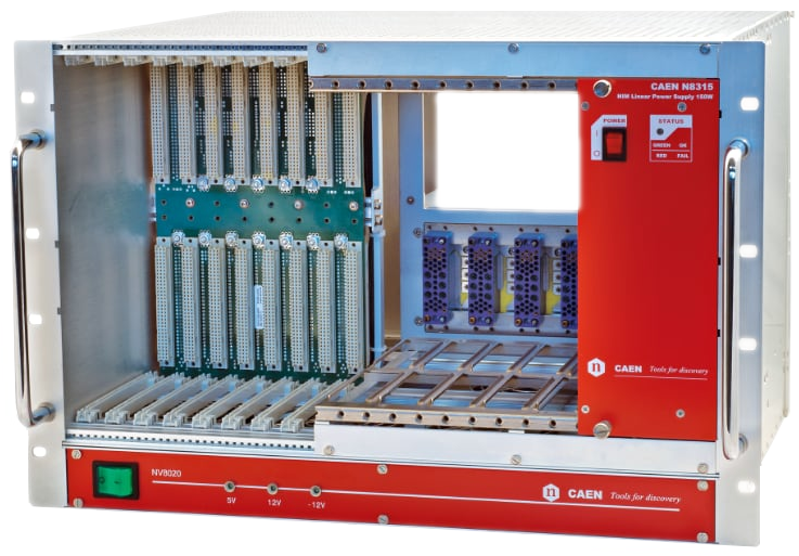
NV8020A
VME8100
VME8011
VME8200
VX1724
A5818
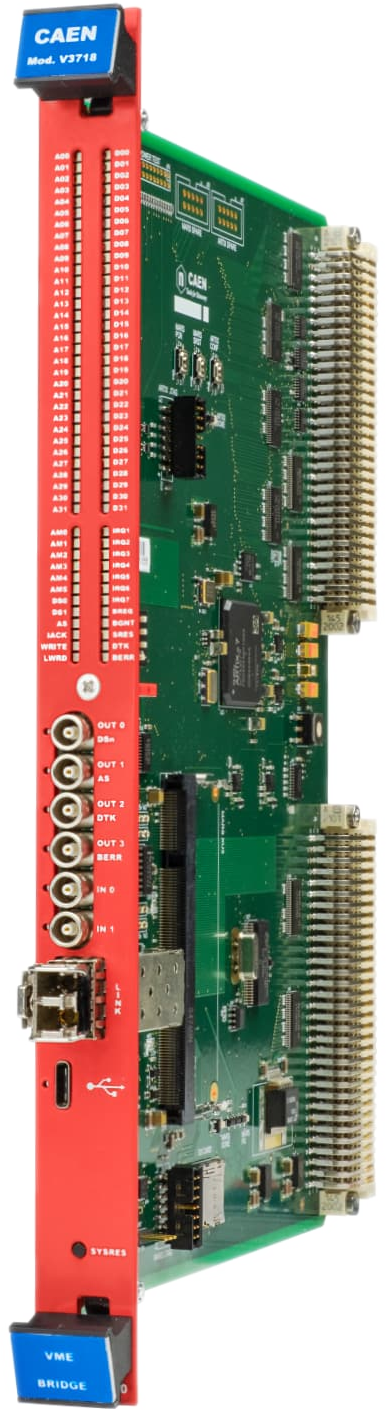
V3718
V4718
VME8004B
VME8004X
VME8008X
Request a Quote

Compare

|
Image
|
Name
|
Package
|
No. of Channels
|
Max Sampling Rate (MS/s)
|
Bandwidth (MHz)
|
Full Scale Range (V)
|
Resolution (bits)
|
Board Memory (Samples/ch)
|
Analog Input Connectors
|
CAEN firmware
|
Open FPGA
|
|
|
VX2730 |
VME64X |
32 |
500 |
250 |
[0.2 ÷ 4] |
14 |
84 M |
MCX |
DPP-PHA, DPP-PSD, D-SCOPE<sup>(cs)</sup> |
YES |
|
|
V1725 / V1725S |
VME |
8 / 16 |
250 |
125 |
0.5 - 2 |
14 |
640 k / 5.12 M |
MCX |
DPP-PHA, DPP-PSD, DPP-ZLEplus, D-WAVE |
NO |
|
|
DT2745 |
Desktop |
64 |
125 |
20 |
[0.04 + 4] |
16 |
21 M |
2mm 40-pin header male |
DPP-PHA, DPP-PSD, D-SCOPE, DPP-ZLEplus<sup>(cs)</sup> |
YES |
|
|
New R5560 |
rack mount 19 -2U |
128+6 |
125 |
60 |
2 |
14 |
max. 8k |
RJ45 |
n. a. |
YES |
|
|
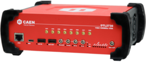
New DTL2730 |
Desktop |
8 |
500 |
TBD |
TBD |
14 |
TBD |
MCX |
DPP-PHA(cs), DPP-PSD(cs), D-SCOPE(cs) |
YES |
|
|
V1761 |
VME |
2 |
4000 |
1000 |
1 |
10 |
7.2 M / 57.6 M |
MCX |
D-WAVE |
NO |
|
|
DT5751 |
Desktop |
2(DES mode) - 4 |
2000(DES mode) - 1000 |
500 |
0.2 / 1 |
10 |
3.6 M(DES mode) - 1.8 M |
MCX |
DPP-PSD, DPP-ZLEplus, D-WAVE |
NO |
|

|
VX1740D |
VME64X |
64 |
62.5 |
30 |
2 / 10 |
12 |
192 k |
SMC 68P |
DPP-QDC, D-WAVE |
NO |
|
|
DT5725 / DT5725S |
Desktop |
8 |
250 |
125 |
0.5 - 2 |
14 |
640 k / 5.12 M |
MCX |
DPP-PHA, DPP-PSD, DPP-ZLEplus, DPP-DAW, D-WAVE |
NO |
|
|
VX1724 |
VME64X |
8 |
100 |
40 |
0.5 / 2.25 / 10 |
14 |
512 k / 4 M |
MCX |
DPP-PHA, DPP-DAW |
NO |
|
|
DT5761 |
Desktop |
1 |
4000 |
1000 |
1 |
10 |
7.2 M |
MCX |
D-WAVE |
NO |
|
|
VX2745 |
VME64X |
64 |
125 |
20 |
[0.4 ÷ 4] |
16 |
21 M |
2mm 40-pin header male |
D-SCOPE, DPP-PHA, DPP-PSD, DPP-ZLEplus<sup>(cs)</sup> |
YES |
|
|
DT5724 |
Desktop |
4 / 2 |
100 |
40 |
0.5 / 2.25 / 10 |
14 |
512 k / 4 M |
MCX |
DPP-PHA, DPP-DAW, D-WAVE |
NO |
|
|
DT5730 / DT5730S |
Desktop |
8 |
500 |
250 |
0.5 - 2 |
14 |
640 k / 5.12 M |
MCX |
DPP-PHA, DPP-PSD, DPP-ZLEplus, DPP-DAW, D-WAVE |
NO |
|
|
VX2740 |
VME64X |
64 |
125 |
50 |
2 |
16 |
21 M |
2mm 40-pin header male |
DPP-PHA, D-SCOPE, DPP-PSD, DPP-ZLEplus<sup>(cs)</sup> |
YES |
|
|
V1724 |
VME |
8 |
100 |
40 |
0.5 / 2.25 / 10 |
14 |
512 k / 4 M |
MCX |
DPP-PHA, DPP-DAW, D-WAVE |
NO |
|
|
VX1761 |
VME64X |
2 |
4000 |
1000 |
1 |
10 |
7.2 M / 57.6 M |
MCX |
D-SCOPE |
NO |
|
|
DT2740 |
Desktop |
64 |
125 |
50 |
2 |
16 |
21 M |
2mm 40-pin header male |
DPP-PHA, DPP-PSD, D-SCOPE, DPP-ZLEplus<sup>(cs)</sup> |
YES |
|
|
V2740 |
VME |
64 |
125 |
50 |
2 |
16 |
21 M |
2mm 40-pin header male |
DPP-PHA, DPP-PSD, D-SCOPE, DPP-ZLEplus<sup>(cs)</sup> |
YES |
|
|
New DT2751 |
Desktop |
16 |
1000 |
500 |
[0.2 ÷ 2] |
14 |
84 M |
MCX |
DPP-PHA, DPP-PSD, D-SCOPE<sup>(cs)</sup> |
YES |
|
|
V1730 / V1730S |
VME |
8 / 16 |
500 |
250 |
0.5 - 2 |
14 |
640 k / 5.12 M |
MCX |
DPP-PHA, DPP-PSD, DPP-ZLEplus, D-WAVE |
NO |
|
|
N6725 / N6725S |
NIM |
8 |
250 |
125 |
0.5 - 2 |
14 |
640 k / 5.12 M |
MCX |
DPP-PHA, DPP-PSD, DPP-ZLEplus, DPP-DAW, D-WAVE |
NO |
|
|
New VX2751 |
VME64X |
16 |
1000 |
500 |
[0.2 ÷ 2] |
14 |
84 M |
MCX |
DPP-PHA, DPP-PSD, D-SCOPE<sup>(cs)</sup> |
YES |
|
|
VX1740 |
VME64X |
64 |
62.5 |
30 |
2 / 10 |
12 |
192 k / 1.5 M |
SMC 68P |
D-WAVE |
NO |
|
|
DT5740D |
Desktop |
32(SMC conn.) - 16(MCX conn) |
62.5 |
30 |
2 / 10 |
12 |
192 k |
SMC 68P - MCX |
DPP-QDC,D-WAVE |
NO |
|
|
V2745 |
VME |
64 |
125 |
20 |
[0.04 + 4] |
16 |
21 M |
2mm 40-pin header male |
DPP-PHA, DPP-PSD, D-SCOPE, DPP-ZLEplus<sup>(cs)</sup> |
YES |
|
|
DT5742 |
Desktop |
16 + 1 |
5000 (Based on DRS4 chip: 5 GS/s Switched Capacitor Array) |
500 |
1 |
12 |
0.128 / 1 |
MCX |
D-WAVE |
NO |
|
|
VX1725 / VX1725S |
VME64X |
8 / 16 |
250 |
125 |
0.5 - 2 |
14 |
640 k / 5.12 M |
MCX |
DPP-PHA, DPP-PSD, DPP-ZLEplus, DPP-DAW, D-WAVE |
NO |
|
|
VX1730 / VX1730S |
VME64X |
8 / 16 |
500 |
250 |
0.5 - 2 |
14 |
640 k / 5.12 M |
MCX |
DPP-PHA, DPP-PSD, DPP-ZLEplus, DPP-DAW, D-WAVE |
NO |
|
|
V2730B |
VME64 |
16 |
500 |
250 |
[0.2 ÷ 4] |
14 |
MCX |
84 M |
DPP-PHA, DPP-PSD, D-SCOPE(cs) |
YES |
|
|
N6730 / N6730S |
NIM |
8 |
500 |
250 |
0.5 - 2 |
14 |
640 k / 5.12 M |
MCX |
DPP-PHA, DPP-PSD, DPP-ZLEplus, DPP-DAW, D-WAVE |
NO |
|
|
V1743 |
VME |
16 |
3200 (Based on SAMLONG chip: 3.2 GS/s Switched Capacitor Array) |
500 |
2.5 |
12 |
0.007 M |
MCX |
D-WAVE |
NO |
|
|
VX1751 |
VME64X |
2(DES mode) - 4 |
2000(DES mode) - 1000 |
500 |
0.2 / 1 |
10 |
3.6 M(DES mode) - 1.8 M / 28.8 M(DES mode) - 14.4 M |
MCX |
DPP-PSD, DPP-ZLEplus, D-WAVE |
NO |
|

|
DT5740 |
Desktop |
32(SMC conn.) - 16(MCX conn) |
62.5 |
30 |
2 / 10 |
12 |
192 k |
SMC 68P - MCX |
D-WAVE |
NO |
|
|
V1720 |
VME |
8 |
250 |
125 |
2 |
12 |
1.25 M / 10 M |
MCX |
DPP-PSD, D-WAVE |
NO |
|
|
V1751 |
VME |
2(DES mode) - 4 |
2000(DES mode) - 1000 |
500 |
0.2 / 1 |
10 |
3.6 M(DES mode) - 1.8 M / 28.8 M(DES mode) - 14.4 M |
MCX |
DPP-PSD, DPP-ZLEplus, D-WAVE |
NO |
|
|
VX1742 |
VME64X |
32 + 2 |
5000 (Based on DRS4 chip: 5 GS/s Switched Capacitor Array) |
500 |
1 |
12 |
0.128 / 1 |
MCX |
D-WAVE |
NO |
|
|
DT5743 |
Desktop |
8 |
3200 (Based on SAMLONG chip: 3.2 GS/s Switched Capacitor Array) |
500 |
2.5 |
12 |
0.007 M |
MCX |
D-WAVE |
NO |
|
|
DT5720 |
Desktop |
4 / 2 |
250 |
125 |
2 |
12 |
1.25 M / 10 M |
MCX |
DPP-PSD, D-WAVE |
NO |
|
|
V1742 |
VME |
32 + 2 |
5000 (Based on DRS4 chip: 5 GS/s Switched Capacitor Array) |
500 |
1 |
12 |
0.128 / 1 |
MCX |
D-WAVE |
NO |
|
|
DT2730 |
Desktop |
32 / 16 |
500 |
250 |
[0.2 ÷ 4] |
14 |
MCX |
84 M |
DPP-PHA, DPP-PSD, D-SCOPE |
YES |
|
|
VX1743 |
VME64X |
16 |
3200 (Based on SAMLONG chip: 3.2 GS/s Switched Capacitor Array) |
500 |
2.5 |
12 |
0.007 M |
MCX |
D-WAVE |
NO |
|
|
V1740D |
VME |
64 |
62.5 |
30 |
2 / 10 |
12 |
192 k |
SMC 68P |
DPP-QDC, D-WAVE |
NO |
|
|
New DTL2751 |
Desktop |
4 |
1000 |
TBD |
TBD |
14 |
MCX |
TBD |
DPP-PSD(cs), D-SCOPE(cs) |
YES |
|
|
VX1720 |
VME64X |
8 |
250 |
125 |
2 |
12 |
1.25 M / 10 M |
MCX |
DPP-PSD, D-WAVE |
NO |
|
|
N6742 |
NIM |
16 + 1 |
5000 (Based on DRS4 chip: 5 GS/s Switched Capacitor Array) |
500 |
1 |
12 |
0.128 / 1 |
MCX |
D-WAVE |
NO |
Technical Specifications
|
GENERAL |
|
|||||||||||
|
ANALOG INPUT |
|
|||||||||||
|
DIGITAL CONVERSION |
*The minimum value may depend on the digitizer model, the firmware, and the hardware downsampling mode. |
|||||||||||
|
SYSTEM PERFORMANCES |
|
|||||||||||
|
DIGITAL I/O |
|
|||||||||||
|
ANALOG OUT |
|
|||||||||||
|
ACQUISITION MEMORY |
|
|||||||||||
|
COMMUNICATION INTERFACE |
|
|||||||||||
|
TRIGGER AND EVENT ACQUISITION |
Trigger Sources
Triggered Mode: all the channels fire simultaneously upon a global trigger generated by the Central Logic Unit receiving the trigger source signals; a zero suppression function is available.
Streaming Readout Mode: each channel autonomously identifies the ROI and uses the local trigger to get events independently on the other channels; validation logics can be configured for correlated acquisition (coincidence/anticoincidence).
|
|||||||||||
|
SYNCHRONIZATION |
|
|||||||||||
|
FPGA |
|
|||||||||||
|
CAEN FIRMWARE |
Upgrades (Free): Web available CFA files for Waveform Recording and DPP firmware upgrade through the CAEN Toolbox software, via VMEbus or Optical Link. Waveform Recording Firmware (Freeware): Designed for waveform recording. DPP Firmware (Shareware): Pay firmware implementing a digital pulse processing algorithm (30-minute per power cycle in Trial mode; license is required for full-time work.):
|
|||||||||||
|
SOFTWARE |
|
|||||||||||
|
ENVIRONMENTAL |
|
|||||||||||
|
REGULATORY COMPLIANCE |
|
|||||||||||
|
POWER CONSUMPTIONS |
+5 V: 4.5 A (Typ.) |
Footer