
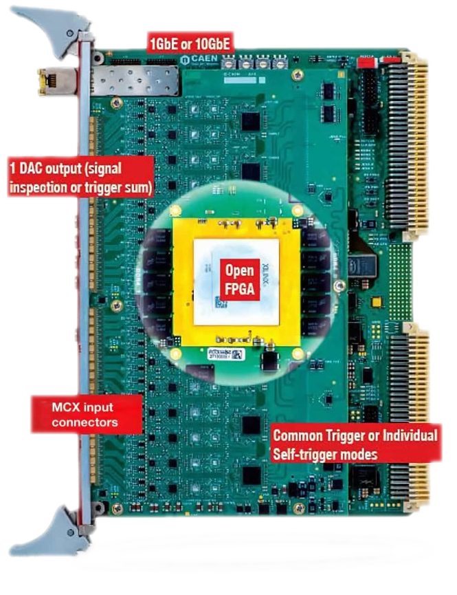
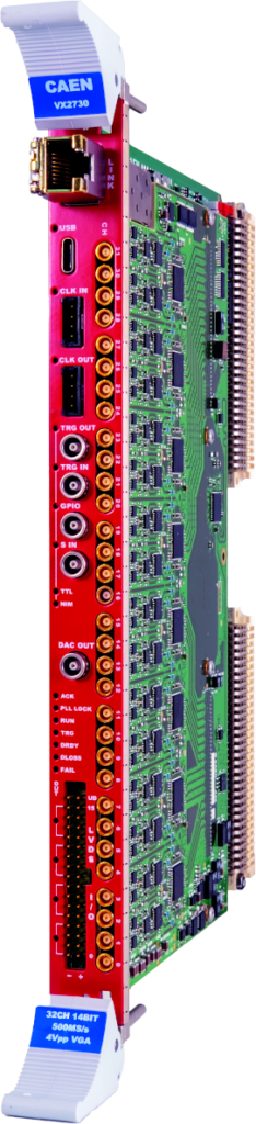
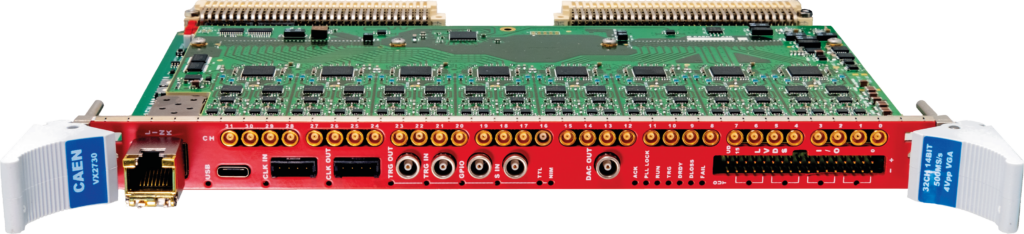
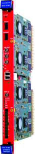
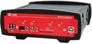
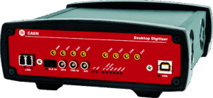
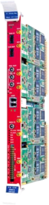
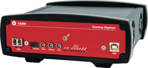
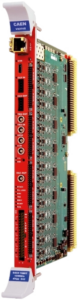
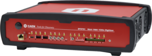
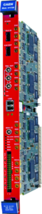
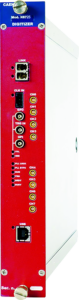
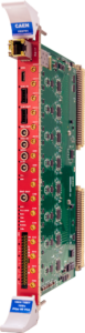
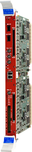
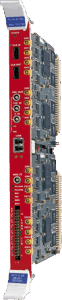
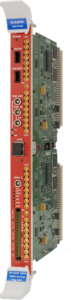
VX2730
32/16 Input Channel 14 bit 500 MS/s Digitizer with Programmable Analog Gain
Highlights
-
32 or 16 independent input channels, 500 MS/s 14-bit, with individual DC offset adjustment and Software selectable analog gain (VGA)
-
Front panel readout via USB-3.0 or 1/10Gb Ethernet
-
On-board Zynq® UltraScale+™ FPGA with embedded Linux-based ARM® processor
-
5GB of total acquisition memory (DDR4)
-
Open FPGA architecture fully supported by SCI-Compiler tool
-
Ready-to-Use Firmware solutions to get time-stamped waveforms and physical quantities (check here for the available options)
-
Triggered and Streaming Readout modes supported
-
System features: Multi-board synchronization, digital I/Os for trigger logic, on-board storage of multiple firmware images, 125MS/s 14-bit DAC output and integrated web interface
-
Software ecosystem:
-
GUI-based readout software available for multiparametric spectroscopy (CoMPASS) or waveform recording (WaveDump2)
-
Firmware/software generator and compiler for the Open FPGA (Sci-Compiler), eliminating the need for FPGA programming skills
-
Libraries (FELib) and demo codes are provided for software customization
-
-
Wide range of applications (from Nuclear and Particle Physics to High Timing Resolution, Fast Neutron Spectroscopy, and Homeland Security)
-
Suited for signals from liquid or inorganic scintillators coupled to PMTs or SiPMs
-
Fully compliant with CAEN μ-crate module
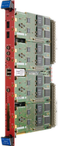
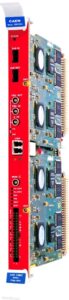
Overview
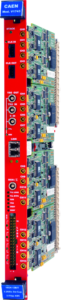
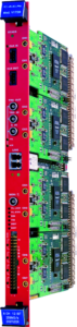
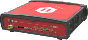
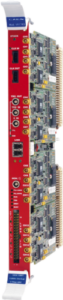
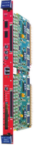
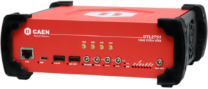
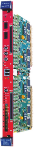
The CAEN mod. VX2730 Digitizer is a 32 or 16 input channel digital signal processor for radiation detectors in the VME64X form factor. It offers not only waveform digitization and recording but also Multi-Channel Analysis for a complete range of applications like nuclear and particle physics, high-timing resolution, Fast Neutron Spectroscopy, and Homeland Security. It is compliant with mid-fast signals typically coming from liquid or inorganic scintillators coupled to PMTs or SiPMs.
Each input channel is able to independently digitize detector signals through a 14-bit ADC at 500 MS/s. Data acquisition is driven by trigger signal generation and the identification of a Region of Interest (ROI), defined in terms of sample count or time duration. Trigger sources can be local (channel self-trigger), external, or software-based. Once acquired, the digitized data is processed within the FPGA, stored in high-speed memory as events—including Trigger ID and Timestamp tags—and then transferred via high-bandwidth communication interfaces for further analysis.
The digitizer supports different acquisition modes, designed to balance throughput, latency, and data efficiency according to experimental requirements:
-
Triggered Mode: All channels acquire data simultaneously upon a global trigger generated by a Central Logic Unit, which processes local triggers from individual channels. External and software triggers can also be configured as sources for the global trigger. Zero suppression algorithms can be applied to remove non-significant data and reduce the readout payload.
-
Streaming Readout Mode: Each channel autonomously identifies its ROI using the self-trigger mechanism, acquiring data independently of the other channels. This mode includes automatic zero suppression (non-triggered channels are not acquired), maximizes acquisition rates, and is ideal for applications requiring real-time parameter extraction. In addition, correlation logics can be configured to validate event acquisition upon coincidences or anticoincidences between local and external triggers.
The VX2730 can operate using both pre-configured firmware developed by CAEN and custom user-generated firmware, offering flexibility for a wide range of applications. Multiple firmware images can be stored simultaneously in the digitizer’s FLASH memory and quickly activated when needed. CAEN provides ready-to-use firmware solutions optimized for specific acquisition and processing needs:
-
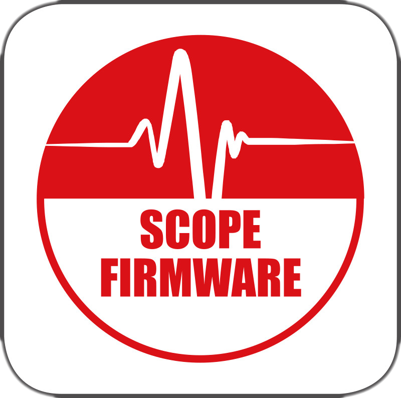
Scope Firmware: Based on full waveform recording in triggered acquisition mode. A zero suppression function is available to reduce unnecessary data readout.
-
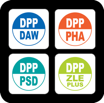
DPP-PSD Firmware: Implements Digital Pulse Processing algorithms for charge integration and pulse shape discrimination. Physical parameters such as pulse height, charge, timestamp, and PSD are extracted from waveforms acquired in streaming readout. It is yet possible to save both raw waves and parameters.
For users requiring custom acquisition and processing, the Open FPGA architecture enables firmware customization through SCI-Compiler. This graphical tool allows users to create personalized firmware solutions without HDL skills. In addition, Sci-Compiler automatically generates drivers and libraries and provides graphical utilities for developing custom DAQ software.
The Linux-based Arm processor embedded in the onboard CPU makes it possible to run automated user routines. Multi-board synchronization can be implemented via backplane or front panel easy-cabling options. Multiple communication interfaces offer flexible readout options: USB 3.0 type-C and 1/10 Gigabit Ethernet.
For detailed information on available firmware for the 2730 family and the structure of programming files (.CUP), please refer to the following page.
This product is compatible with the following third-party software:
Moreover, you can check this FAQ to see which CAEN VME crates are suitable for this product.
Software

CAEN Toolbox

COMPASS
Sci-Compiler
Graphical Programming Language for CAEN Open FPGA Boards

CAEN FELib Library
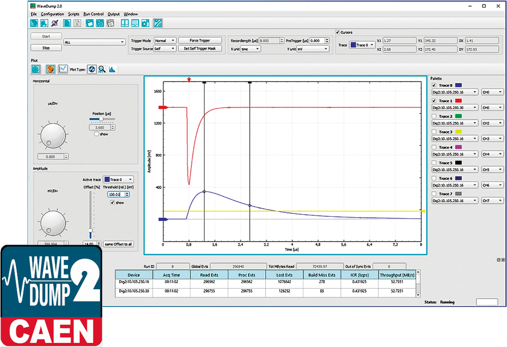
WAVEDUMP2
Open Source Software for Digitizer 2.0 and 1.0 Series


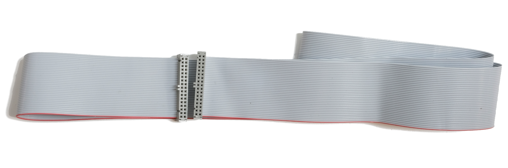
Accessories
A954
A316
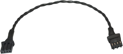
A319A
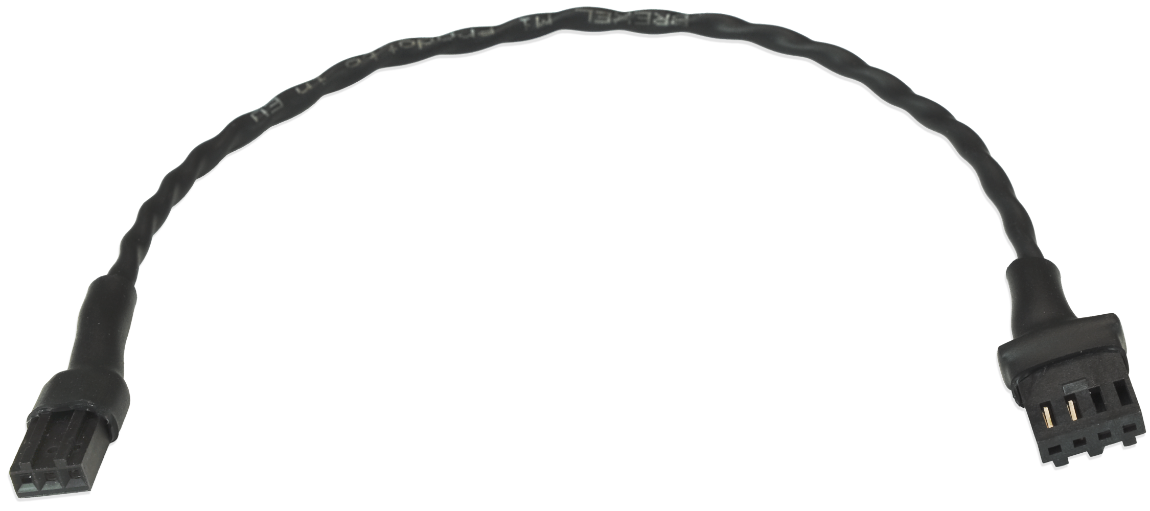
A319B
A952
Cable assembly 2.54mm 34 pin female to 2.54mm 34 pin female - 50 cm
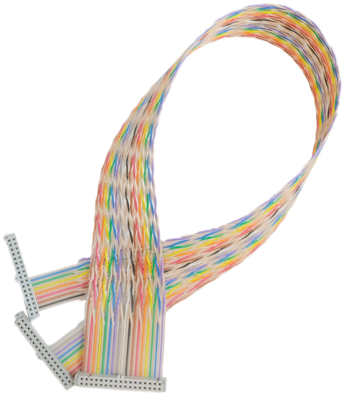
A953
Cable assembly 2.54mm 34 pin female to two 2.54mm 34 pin female – 50 cm
Request a Quote

Compare

|
Image
|
Name
|
Package
|
No. of Channels
|
Max Sampling Rate (MS/s)
|
Bandwidth (MHz)
|
Full Scale Range (V)
|
Resolution (bits)
|
Board Memory (Samples/ch)
|
Analog Input Connectors
|
CAEN firmware
|
Open FPGA
|
|
|
VX2730 |
VME64X |
32 |
500 |
250 |
[0.2 ÷ 4] |
14 |
84 M |
MCX |
DPP-PHA, DPP-PSD, D-SCOPE<sup>(cs)</sup> |
YES |
|
|
V1725 / V1725S |
VME |
8 / 16 |
250 |
125 |
0.5 - 2 |
14 |
640 k / 5.12 M |
MCX |
DPP-PHA, DPP-PSD, DPP-ZLEplus, D-WAVE |
NO |
|
|
DT2745 |
Desktop |
64 |
125 |
20 |
[0.04 + 4] |
16 |
21 M |
2mm 40-pin header male |
DPP-PHA, DPP-PSD, D-SCOPE, DPP-ZLEplus<sup>(cs)</sup> |
YES |
|
|
New R5560 |
rack mount 19 -2U |
128+6 |
125 |
60 |
2 |
14 |
max. 8k |
RJ45 |
n. a. |
YES |
|
|
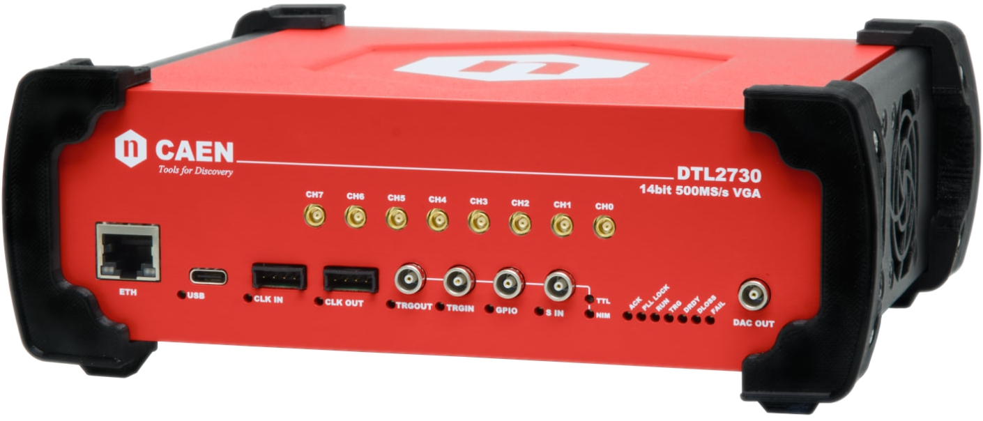
New DTL2730 |
Desktop |
8 |
500 |
TBD |
TBD |
14 |
TBD |
MCX |
DPP-PHA(cs), DPP-PSD(cs), D-SCOPE(cs) |
YES |
|
|
V1761 |
VME |
2 |
4000 |
1000 |
1 |
10 |
7.2 M / 57.6 M |
MCX |
D-WAVE |
NO |
|
|
DT5751 |
Desktop |
2(DES mode) - 4 |
2000(DES mode) - 1000 |
500 |
0.2 / 1 |
10 |
3.6 M(DES mode) - 1.8 M |
MCX |
DPP-PSD, DPP-ZLEplus, D-WAVE |
NO |
|

|
VX1740D |
VME64X |
64 |
62.5 |
30 |
2 / 10 |
12 |
192 k |
SMC 68P |
DPP-QDC, D-WAVE |
NO |
|
|
DT5725 / DT5725S |
Desktop |
8 |
250 |
125 |
0.5 - 2 |
14 |
640 k / 5.12 M |
MCX |
DPP-PHA, DPP-PSD, DPP-ZLEplus, DPP-DAW, D-WAVE |
NO |
|
|
VX1724 |
VME64X |
8 |
100 |
40 |
0.5 / 2.25 / 10 |
14 |
512 k / 4 M |
MCX |
DPP-PHA, DPP-DAW |
NO |
|
|
DT5761 |
Desktop |
1 |
4000 |
1000 |
1 |
10 |
7.2 M |
MCX |
D-WAVE |
NO |
|
|
VX2745 |
VME64X |
64 |
125 |
20 |
[0.4 ÷ 4] |
16 |
21 M |
2mm 40-pin header male |
D-SCOPE, DPP-PHA, DPP-PSD, DPP-ZLEplus<sup>(cs)</sup> |
YES |
|
|
DT5724 |
Desktop |
4 / 2 |
100 |
40 |
0.5 / 2.25 / 10 |
14 |
512 k / 4 M |
MCX |
DPP-PHA, DPP-DAW, D-WAVE |
NO |
|
|
DT5730 / DT5730S |
Desktop |
8 |
500 |
250 |
0.5 - 2 |
14 |
640 k / 5.12 M |
MCX |
DPP-PHA, DPP-PSD, DPP-ZLEplus, DPP-DAW, D-WAVE |
NO |
|
|
VX2740 |
VME64X |
64 |
125 |
50 |
2 |
16 |
21 M |
2mm 40-pin header male |
DPP-PHA, D-SCOPE, DPP-PSD, DPP-ZLEplus<sup>(cs)</sup> |
YES |
|
|
V1724 |
VME |
8 |
100 |
40 |
0.5 / 2.25 / 10 |
14 |
512 k / 4 M |
MCX |
DPP-PHA, DPP-DAW, D-WAVE |
NO |
|
|
VX1761 |
VME64X |
2 |
4000 |
1000 |
1 |
10 |
7.2 M / 57.6 M |
MCX |
D-SCOPE |
NO |
|
|
DT2740 |
Desktop |
64 |
125 |
50 |
2 |
16 |
21 M |
2mm 40-pin header male |
DPP-PHA, DPP-PSD, D-SCOPE, DPP-ZLEplus<sup>(cs)</sup> |
YES |
|
|
V2740 |
VME |
64 |
125 |
50 |
2 |
16 |
21 M |
2mm 40-pin header male |
DPP-PHA, DPP-PSD, D-SCOPE, DPP-ZLEplus<sup>(cs)</sup> |
YES |
|
|
New DT2751 |
Desktop |
16 |
1000 |
500 |
[0.2 ÷ 2] |
14 |
84 M |
MCX |
DPP-PHA, DPP-PSD, D-SCOPE<sup>(cs)</sup> |
YES |
|
|
V1730 / V1730S |
VME |
8 / 16 |
500 |
250 |
0.5 - 2 |
14 |
640 k / 5.12 M |
MCX |
DPP-PHA, DPP-PSD, DPP-ZLEplus, D-WAVE |
NO |
|
|
N6725 / N6725S |
NIM |
8 |
250 |
125 |
0.5 - 2 |
14 |
640 k / 5.12 M |
MCX |
DPP-PHA, DPP-PSD, DPP-ZLEplus, DPP-DAW, D-WAVE |
NO |
|
|
New VX2751 |
VME64X |
16 |
1000 |
500 |
[0.2 ÷ 2] |
14 |
84 M |
MCX |
DPP-PHA, DPP-PSD, D-SCOPE<sup>(cs)</sup> |
YES |
|
|
VX1740 |
VME64X |
64 |
62.5 |
30 |
2 / 10 |
12 |
192 k / 1.5 M |
SMC 68P |
D-WAVE |
NO |
|
|
DT5740D |
Desktop |
32(SMC conn.) - 16(MCX conn) |
62.5 |
30 |
2 / 10 |
12 |
192 k |
SMC 68P - MCX |
DPP-QDC,D-WAVE |
NO |
|
|
V2745 |
VME |
64 |
125 |
20 |
[0.04 + 4] |
16 |
21 M |
2mm 40-pin header male |
DPP-PHA, DPP-PSD, D-SCOPE, DPP-ZLEplus<sup>(cs)</sup> |
YES |
|
|
DT5742 |
Desktop |
16 + 1 |
5000 (Based on DRS4 chip: 5 GS/s Switched Capacitor Array) |
500 |
1 |
12 |
0.128 / 1 |
MCX |
D-WAVE |
NO |
|
|
VX1725 / VX1725S |
VME64X |
8 / 16 |
250 |
125 |
0.5 - 2 |
14 |
640 k / 5.12 M |
MCX |
DPP-PHA, DPP-PSD, DPP-ZLEplus, DPP-DAW, D-WAVE |
NO |
|
|
VX1730 / VX1730S |
VME64X |
8 / 16 |
500 |
250 |
0.5 - 2 |
14 |
640 k / 5.12 M |
MCX |
DPP-PHA, DPP-PSD, DPP-ZLEplus, DPP-DAW, D-WAVE |
NO |
|
|
V2730B |
VME64 |
16 |
500 |
250 |
[0.2 ÷ 4] |
14 |
MCX |
84 M |
DPP-PHA, DPP-PSD, D-SCOPE(cs) |
YES |
|
|
N6730 / N6730S |
NIM |
8 |
500 |
250 |
0.5 - 2 |
14 |
640 k / 5.12 M |
MCX |
DPP-PHA, DPP-PSD, DPP-ZLEplus, DPP-DAW, D-WAVE |
NO |
|
|
V1743 |
VME |
16 |
3200 (Based on SAMLONG chip: 3.2 GS/s Switched Capacitor Array) |
500 |
2.5 |
12 |
0.007 M |
MCX |
D-WAVE |
NO |
|
|
VX1751 |
VME64X |
2(DES mode) - 4 |
2000(DES mode) - 1000 |
500 |
0.2 / 1 |
10 |
3.6 M(DES mode) - 1.8 M / 28.8 M(DES mode) - 14.4 M |
MCX |
DPP-PSD, DPP-ZLEplus, D-WAVE |
NO |
|

|
DT5740 |
Desktop |
32(SMC conn.) - 16(MCX conn) |
62.5 |
30 |
2 / 10 |
12 |
192 k |
SMC 68P - MCX |
D-WAVE |
NO |
|
|
V1720 |
VME |
8 |
250 |
125 |
2 |
12 |
1.25 M / 10 M |
MCX |
DPP-PSD, D-WAVE |
NO |
|
|
V1751 |
VME |
2(DES mode) - 4 |
2000(DES mode) - 1000 |
500 |
0.2 / 1 |
10 |
3.6 M(DES mode) - 1.8 M / 28.8 M(DES mode) - 14.4 M |
MCX |
DPP-PSD, DPP-ZLEplus, D-WAVE |
NO |
|
|
VX1742 |
VME64X |
32 + 2 |
5000 (Based on DRS4 chip: 5 GS/s Switched Capacitor Array) |
500 |
1 |
12 |
0.128 / 1 |
MCX |
D-WAVE |
NO |
|
|
DT5743 |
Desktop |
8 |
3200 (Based on SAMLONG chip: 3.2 GS/s Switched Capacitor Array) |
500 |
2.5 |
12 |
0.007 M |
MCX |
D-WAVE |
NO |
|
|
DT5720 |
Desktop |
4 / 2 |
250 |
125 |
2 |
12 |
1.25 M / 10 M |
MCX |
DPP-PSD, D-WAVE |
NO |
|
|
V1742 |
VME |
32 + 2 |
5000 (Based on DRS4 chip: 5 GS/s Switched Capacitor Array) |
500 |
1 |
12 |
0.128 / 1 |
MCX |
D-WAVE |
NO |
|
|
DT2730 |
Desktop |
32 / 16 |
500 |
250 |
[0.2 ÷ 4] |
14 |
MCX |
84 M |
DPP-PHA, DPP-PSD, D-SCOPE |
YES |
|
|
VX1743 |
VME64X |
16 |
3200 (Based on SAMLONG chip: 3.2 GS/s Switched Capacitor Array) |
500 |
2.5 |
12 |
0.007 M |
MCX |
D-WAVE |
NO |
|
|
V1740D |
VME |
64 |
62.5 |
30 |
2 / 10 |
12 |
192 k |
SMC 68P |
DPP-QDC, D-WAVE |
NO |
|
|
New DTL2751 |
Desktop |
4 |
1000 |
TBD |
TBD |
14 |
MCX |
TBD |
DPP-PSD(cs), D-SCOPE(cs) |
YES |
|
|
VX1720 |
VME64X |
8 |
250 |
125 |
2 |
12 |
1.25 M / 10 M |
MCX |
DPP-PSD, D-WAVE |
NO |
|
|
N6742 |
NIM |
16 + 1 |
5000 (Based on DRS4 chip: 5 GS/s Switched Capacitor Array) |
500 |
1 |
12 |
0.128 / 1 |
MCX |
D-WAVE |
NO |
Technical Specifications
|
GENERAL |
|
|||||||||
|
ANALOG INPUT |
|
|||||||||
|
DIGITAL CONVERSION |
|
|||||||||
|
SYSTEM PERFORMANCE |
|
|||||||||
|
DIGITAL I/O |
|
|||||||||
|
ANALOG OUT |
|
|||||||||
|
ACQUISITION MEMORY |
1 Value referred to the Scope firmware (minimum of two buffers admitted) |
|||||||||
|
COMMUNICATION INTERFACES |
|
|||||||||
|
TRIGGER AND EVENT ACQUISITION |
|
|||||||||
|
SYNCHRONIZATION |
|
|||||||||
|
FPGA |
|
|||||||||
|
CAEN FIRMWARE |
Developed by CAEN, stored in the on-board FLASH memory, and live rebootable by Web Interface.
|
|||||||||
|
USER FIRMWARE (OPEN FPGA) |
Sci-Compiler (Shareware) Pay graphical tool for User Firmware generation and compiling with CAEN Programmable Boards.
|
|||||||||
|
SOFTWARE |
|
|||||||||
|
ENVIRONMENTAL |
|
|||||||||
|
REGULATORY COMPLIANCE |
|
|||||||||
|
POWER REQUIREMENTS |
+12V: 0.5 A (Typ.) The values above are preliminary and referred to a 1-GbE Scope firmware; they are subject to change depending on the firmware type. |
Footer