
• Skip to main content
  • Skip to footer
CAEN logo light
  • About
    • Company Profile
    • Our policy
    • Sales network
    • Innovative Projects
    • Careers
    • How to reach us
  • Products
  • Resources
    • Documentation
    • Download
    • FAQ
    • Glossary
    • Certifications
    • Legal and Compliance
  • Support
  • Contact
All productsSpecial OffersForm FactorEducationalPower SupplyModular Pulse ProcessingDigitizer FamiliesFERS FamiliesDigital SpectroscopyCAEN SyS productsFirmware & SoftwarePowered CratesAccessoriesBrands
Background image

V2745

64 Channel 16 bit 125 MS/s Digitizer with Programmable Input Gain
Request a Quote Add to WishlistView Wishlist

Home Modular Pulse Processing ElectronicsAnalogDigitizers V2745

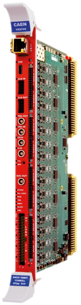
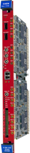
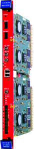
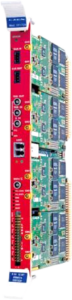
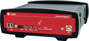
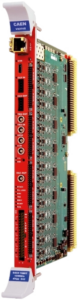
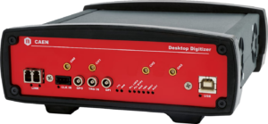
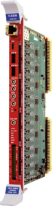
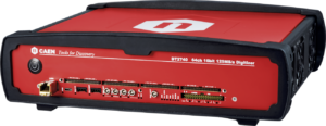
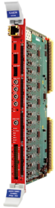
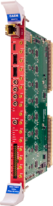
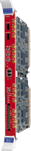
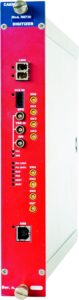
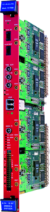
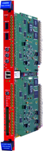
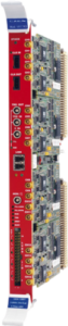
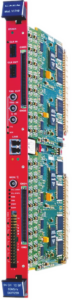
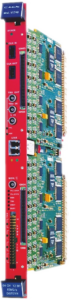
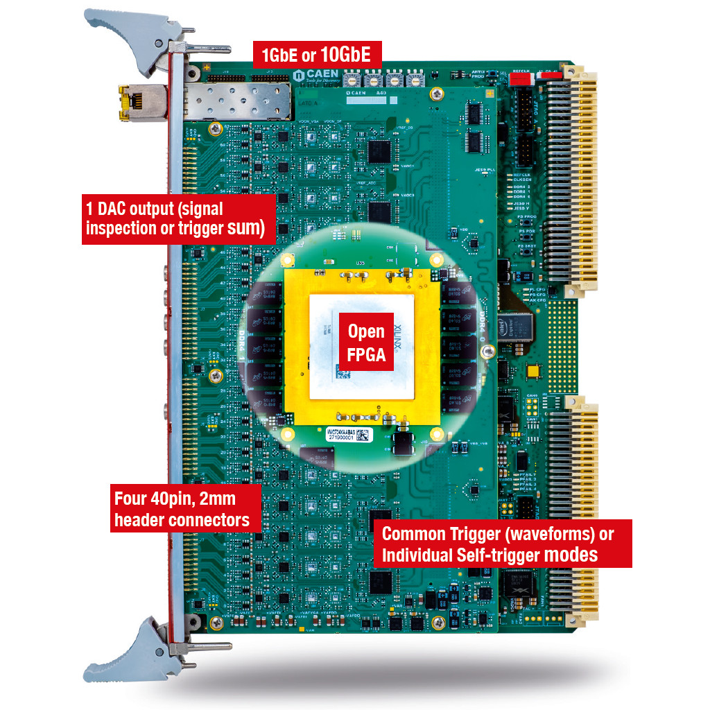
Photo of V2745
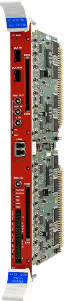
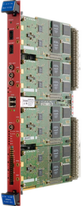
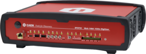
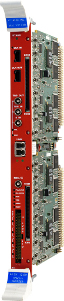
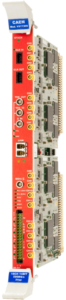
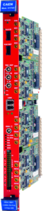
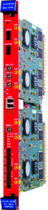
Photo of V2745
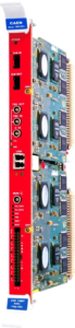
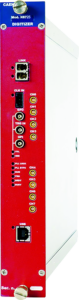
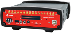
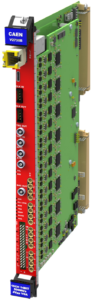
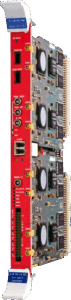
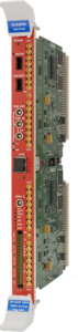
Photo of V2745
DatasheetDownloadCompareTech. Spec.

Highlights

  • 16 bit @ 125 MS/s ADC

  • 64 analog inputs, differential or single-ended, on four 2mm 40-pin header connectors

  • Software selectable Analog Gain up to x100

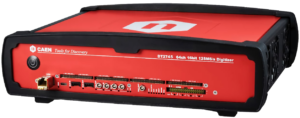
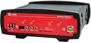
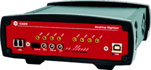
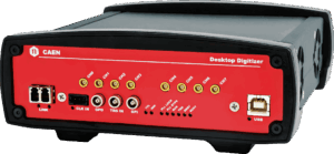
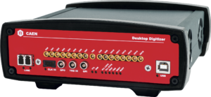
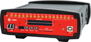
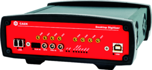
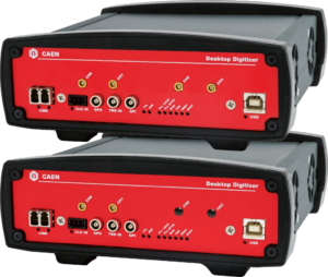
  • DT2745 desktop form factor also available

  • Open FPGA programming through graphical tool SCI-Compiler

  • Wide range of applications (from Neutrino Physics & Dark Matter to Nuclear and Particle Physics to Spectroscopic Imaging)

  • Suited for signals from Semiconductor Detectors coupled with CSPs (Si, HPGe) or scintillators coupled with PMTs (NaI, CsI)

  • On-board firmware selection for different acquisition modes:

    • Scope mode (simultaneous raw waveform acquisition on common trigger)

    • DPP-PHA mode (pulse height and time acquisition on independent channel self-triggers)

    • DPP-PSD mode (pulse shape discrimination and time acquisition on independent channel self-triggers)

    • Predisposition for other algorithms like zero suppression and data reduction

  • Multi-board synchronization and system building capabilities

  • Front panel fully programmable I/Os (4 LEMO TTL/NIM and 16 LVDS)

  • Special 125MS/s 14bit DAC output (LEMO) for signal inspection or trigger sum

  • On-board Xilinx Zynq® UltraScale+™ FPGA with embedded Linux-based ARM processor

  • 2.5GB of Total Acquisition memory (DDR4)

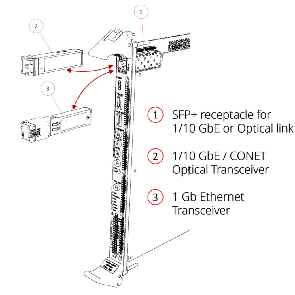
  • Front panel readout via USB-3.0 or 1/10Gb Ethernet

  • Fully supported by CoMPASS and WaveDump2 readout software

  • SDK for embedded Arm and host PC

  • Open FPGA

Overview

The Mod. V2745 Digitizer is a 64-channel digital signal processor for radiation detectors in a VME64X form factor. It offers not only waveform digitization and recording but also Multi-Channel Analysis for nuclear spectroscopy using Silicon strip, segmented HPGe, Scintillation detector with PMTs, Wire Chambers, and others.
The V2745 can perform pulse height measurements (PHA), and other algorithms that will be gradually developed, such as constant fraction timing (CFD), charge integration (QDC) and pulse shape discrimination (PSD). Algorithm settings can be set independently channel by channel.. The input channels with software selectable analog gain up to x100 are provided as differential (on V2745 versions) or single-ended (on V2745B version).
Each channel of the module digitizes the analog input, that can be the signal coming from a physics detector, with a 16 bit, 125 MS/s ADC. The sampled data are used to initiate the digital pulse processing sequence, managed in the FPGA at the firmware level. Different firmware types can be selected via software, according to the specific setup and acquisition mode.

  • Common trigger: all channels acquire simultaneously with a common trigger. The trigger can be fed externally or generated by a combination of individual channel discriminators. This mode is mainly intended for the acquisition of waveforms, like a digital oscilloscope. Options for zero suppression are available to remove not significant data.

  • Independent trigger: suited for trigger-less applications, where no global trigger is needed but each channel acquires waveforms upon its self-trigger which fires through a digital discriminator, independently of the others.

  • DPP: real-time processing in the FPGA allows for the extraction of physical parameters from the waveform (e.g. pulse height, charge, timestamp, PSD), well suited for high counting rate applications. It is yet possible to save both raw waves and parameters.

A template of the firmware is available for customers who want to personalize the acquisition to implement custom algorithms for pulse processing in the open FPGA. The user can have control of the data output information and customize the trigger logic to get several combinations of self-triggers and I/O signals to validate or discard the events.
Custom software can run on the onboard CPU for data reduction and analysis. Multi-board synchronization can be implemented via backplane or front panel easy-cabling options.
Multiple communication interfaces offer flexible readout options: USB 3.0 type-C and 1/10 Gigabit Ethernet.

Supported third-party software:

  • SOLARIS DAQ

  • PKUCAENDAQ

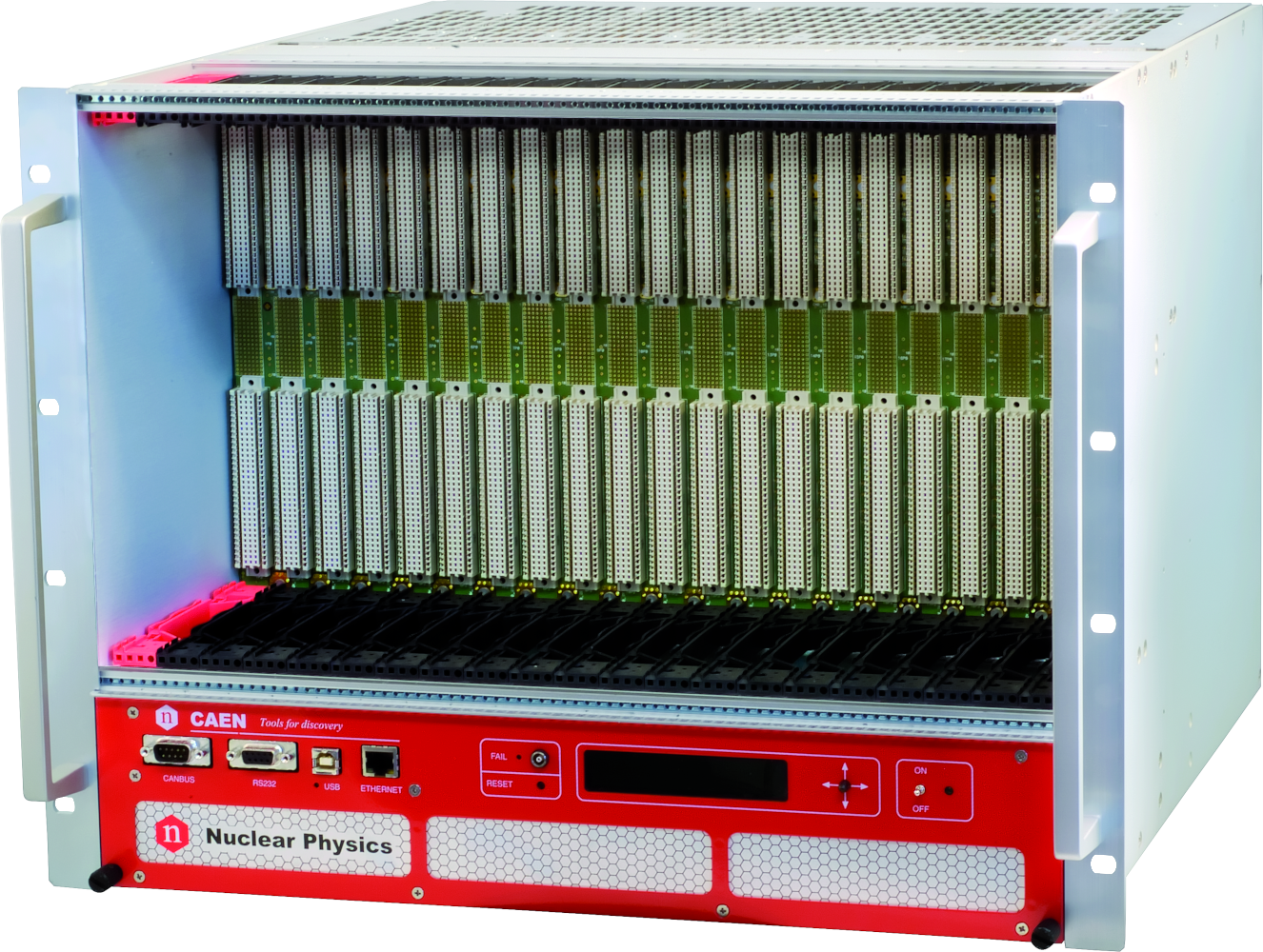
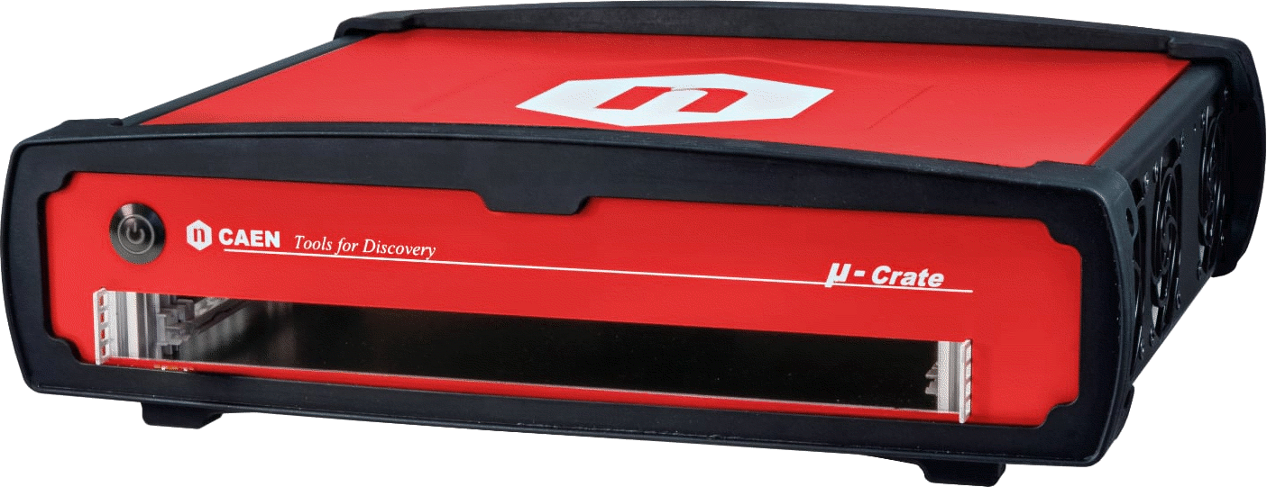
The V2745 fits in the single-slot CAEN VME64X u-crate, which allows you to convert the VME digitizer into a desktop board for lab tests.

Moreover, you can check this FAQ to see which CAEN VME crates are suitable for this product.

Supported Software and Firmware

Software

  • CAEN Toolbox — Multi-Functional Software Suite for the Upgrade of Front-end Boards, Bridges and Power Supplies
  • COMPASS — Multiparametric DAQ Software for Physics Applications
  • Sci-Compiler — Graphical Programming Language for CAEN Open FPGA Boards
  • WaveDump — Readout Application for CAEN Digitizer 1.0
  • CAEN FELib Library — High level library for CAEN Digitizers 2.0

Firmware

  • D-SCOPE — Digitizer 2.0 Waveform Recording Firmware
  • DPP-PSD — Digital Pulse Processing for Charge Integration and Pulse Shape Discrimination
  • DPP-PHA — Digital Pulse Processing for the Pulse Height Analysis
  • DPP-SUP — Super Licence for CAEN Digitizers

Accessories

A954

A954

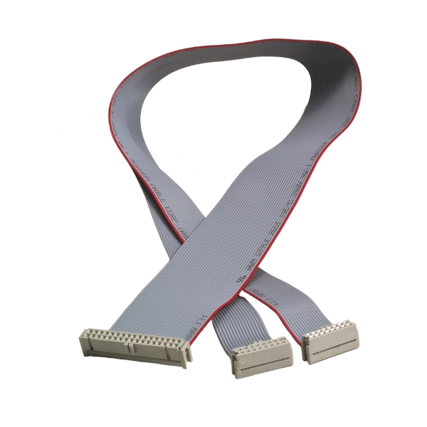
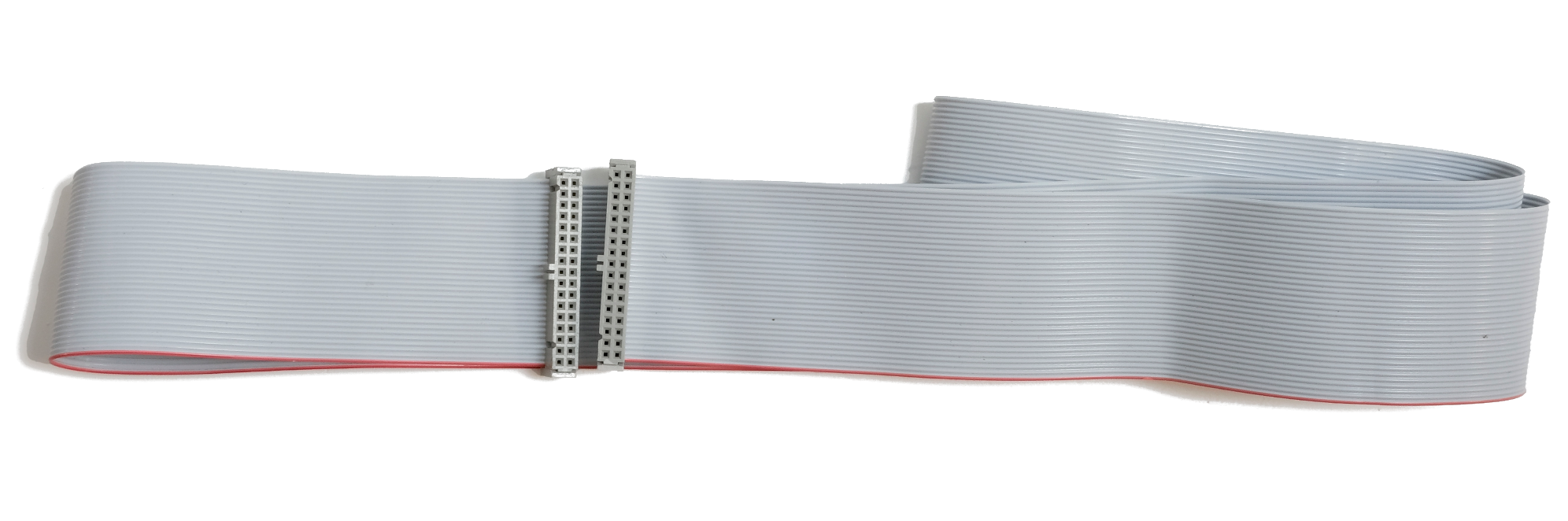
Cable assembly 2.54mm 34 pin female to two 2.54mm 16 pin female - 50 cm
A316

A316

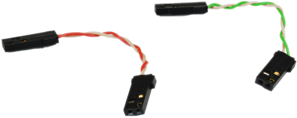
Cable assembly 2.54mm 2-pin header female - 5 cm
DT4700

DT4700

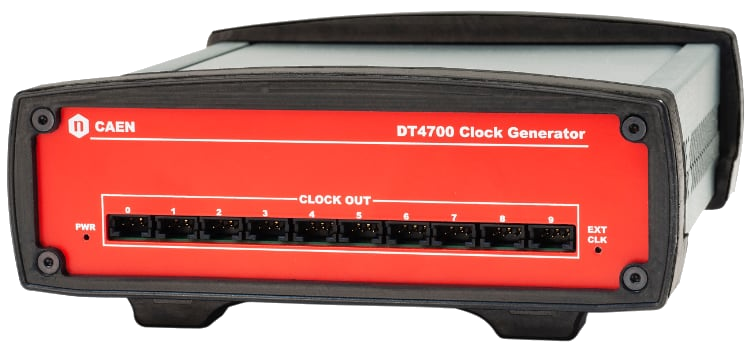
Clock Generator and FAN-OUT
A319A

A319A

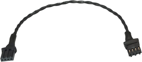
Clock & Sync cable assembly for Digitizer Series 2.0 - 20 cm
A319B

A319B

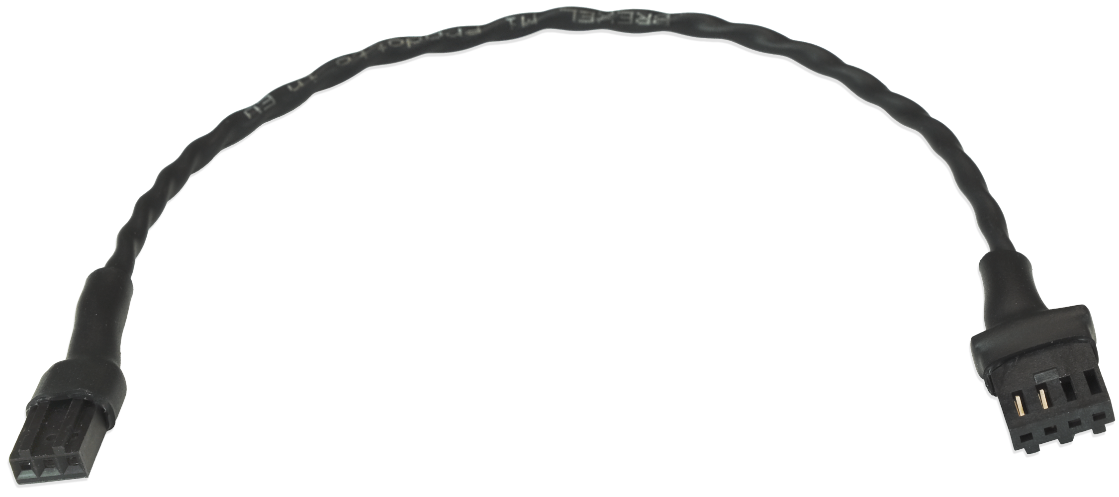
Clock cable assembly from Digitizer Series 1.0 to Digitizer Series 2.0 - 20cm
A372F

A372F

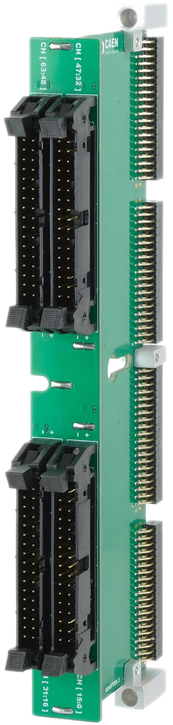
64 channel 2.54mm Male Header Connector Adapter for 274x Digitizers
A372M

A372M

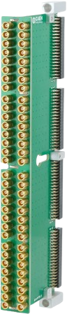
64 channel MCX Coax Connector Adapter for SE signals
A952

A952

Cable assembly 2.54mm 34 pin female to 2.54mm 34 pin female - 50 cm
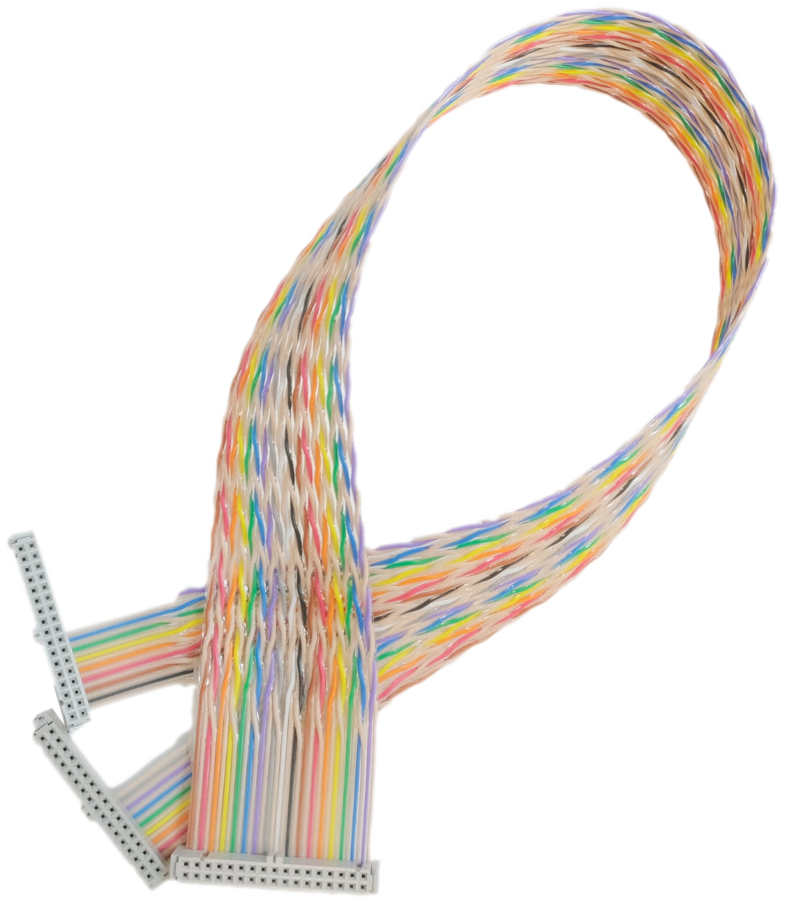
A953

A953

Cable assembly 2.54mm 34 pin female to two 2.54mm 34 pin female – 50 cm
Ordering Options

Code Description
WV2745BXAAAA

V2745B – 64 Ch. 16 bit 125 MS/s Digitizer with Programmable Input Gain, SE

RoHS
WV2745XAAAAA

V2745 – 64 Ch. 16 bit 125 MS/s Digitizer with Programmable Input Gain, Diff

RoHS

You also may be interested in…

µ-crate

µ-crate

Desktop single-slot VME64X Crate
VME8100

VME8100

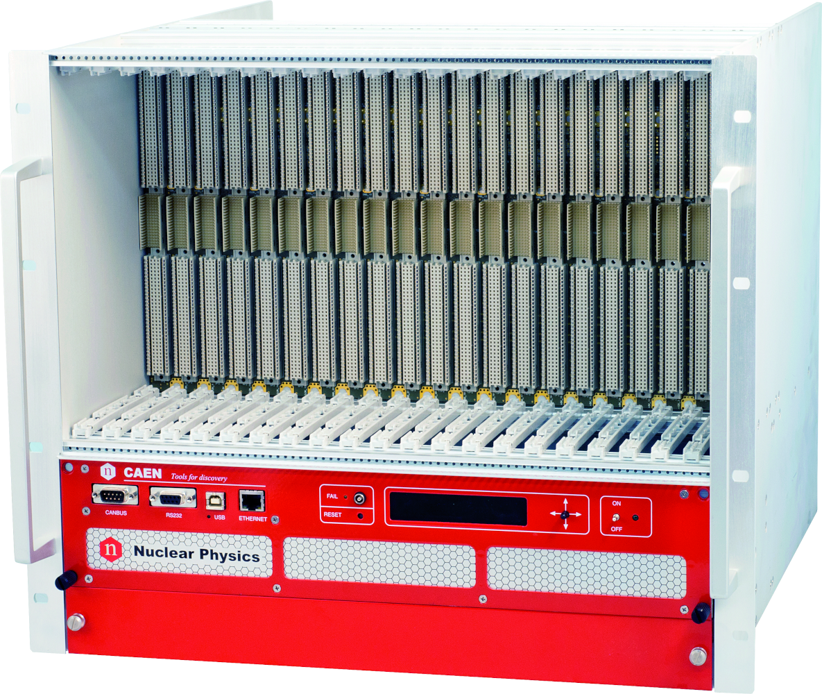
8U 21 Slot VME64/64X Enhanced Crate Series
VME8200

VME8200

9U 21Slot VME64X Enhanced Crate series
VME8004X

VME8004X

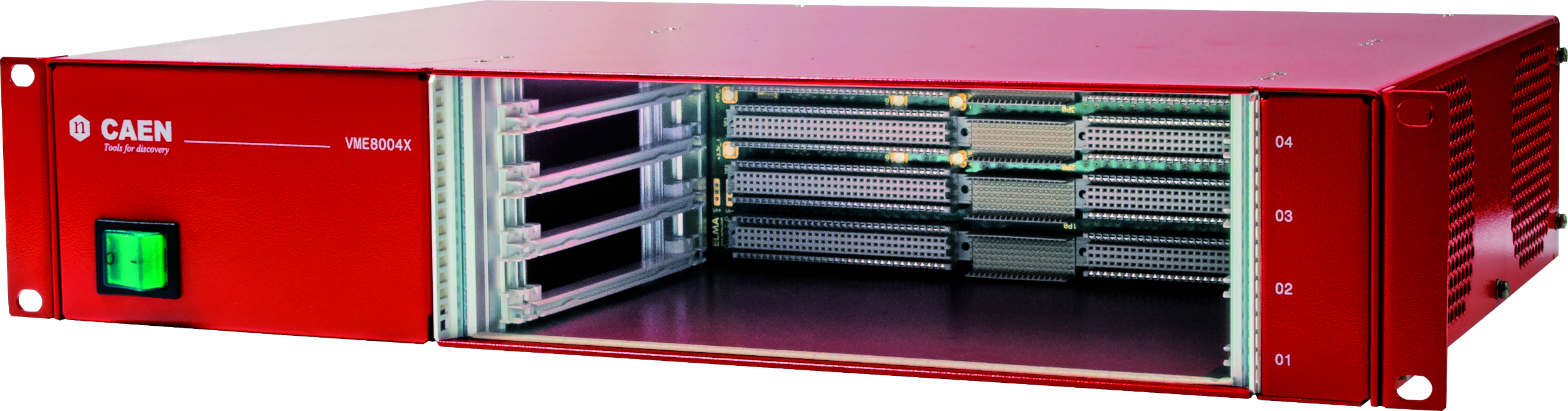
2U 4 Slot VME64X Mini Crate
VME8008X

VME8008X

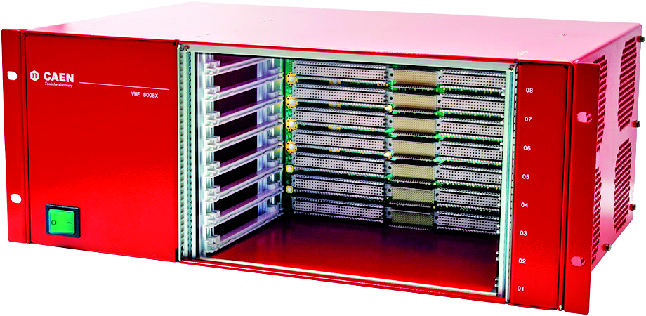
4U 8 Slot VME64X Mini Crate
Download Compare Tech. Spec.

Add to Wishlist
This product is already in your Wishlist
Browse the Wishlist

Request a Quote

Request a Quote

    Submit

    Compare

    Close
    Image
    Name
    Resolution (bits)
    Max Sampling Rate (MS/s)
    No. of Channels
    Package
    Bandwidth (MHz)
    Full Scale Range (V)
    Board Memory (Samples/ch)
    Analog Input Connectors
    CAEN firmware
    Open FPGA
    VX2730

    VX2730

    14

    500

    32

    VME64X

    250

    [0.2 ÷ 4]

    84 M

    MCX

    DPP-PHA, DPP-PSD, D-SCOPE (cs)

    YES

    V1725 / V1725S

    V1725 / V1725S

    14

    250

    8 / 16

    VME

    125

    0.5 - 2

    640 k / 5.12 M

    MCX

    DPP-PHA, DPP-PSD, DPP-ZLEplus, D-WAVE

    NO

    DT2745

    DT2745

    16

    125

    64

    Desktop

    20

    [0.04 + 4]

    21 M

    2mm 40-pin header male

    DPP-PHA, DPP-PSD, D-SCOPE, DPP-ZLEplus<sup>(cs)</sup>

    YES

    R5560
    New

    R5560

    14

    125

    128+6

    rack mount 19 -2U

    60

    2

    max. 8k

    RJ45

    n. a.

    YES

    DTL2730
    New

    DTL2730

    14

    500

    8

    Desktop

    TBD

    TBD

    MCX

    DPP-PHA(cs), DPP-PSD(cs), D-SCOPE(cs)

    YES

    V1761

    V1761

    10

    4000

    2

    VME

    1000

    1

    7.2 M / 57.6 M

    MCX

    D-WAVE

    NO

    DT5751

    DT5751

    10

    2000(DES mode) - 1000

    2(DES mode) - 4

    Desktop

    500

    0.2 / 1

    3.6 M(DES mode) - 1.8 M

    MCX

    DPP-PSD, DPP-ZLEplus, D-WAVE

    NO

    VX1740D

    VX1740D

    12

    62.5

    64

    VME64X

    30

    2 / 10

    192 k

    SMC 68P

    DPP-QDC, D-WAVE

    NO

    DT5725 / DT5725S

    DT5725 / DT5725S

    14

    250

    8

    Desktop

    125

    0.5 - 2

    640 k / 5.12 M

    MCX

    DPP-PHA, DPP-PSD, DPP-ZLEplus, DPP-DAW, D-WAVE

    NO

    VX1724

    VX1724

    14

    100

    8

    VME64X

    40

    0.5 / 2.25 / 10

    512 k / 4 M

    MCX

    DPP-PHA, DPP-DAW

    NO

    DT5761

    DT5761

    10

    4000

    1

    Desktop

    1000

    1

    7.2 M

    MCX

    D-WAVE

    NO

    VX2745

    VX2745

    16

    125

    64

    VME64X

    20

    [0.4 ÷ 4]

    21 M

    2mm 40-pin header male

    D-SCOPE, DPP-PHA, DPP-PSD, DPP-ZLEplus<sup>(cs)</sup>

    YES

    DT5724

    DT5724

    14

    100

    4 / 2

    Desktop

    40

    0.5 / 2.25 / 10

    512 k / 4 M

    MCX

    DPP-PHA, DPP-DAW, D-WAVE

    NO

    DT5730 / DT5730S

    DT5730 / DT5730S

    14

    500

    8

    Desktop

    250

    0.5 - 2

    640 k / 5.12 M

    MCX

    DPP-PHA, DPP-PSD, DPP-ZLEplus, DPP-DAW, D-WAVE

    NO

    VX2740

    VX2740

    16

    125

    64

    VME64X

    50

    2

    21 M

    2mm 40-pin header male

    DPP-PHA, D-SCOPE, DPP-PSD, DPP-ZLEplus<sup>(cs)</sup>

    YES

    V1724

    V1724

    14

    100

    8

    VME

    40

    0.5 / 2.25 / 10

    512 k / 4 M

    MCX

    DPP-PHA, DPP-DAW, D-WAVE

    NO

    VX1761

    VX1761

    10

    4000

    2

    VME64X

    1000

    1

    7.2 M / 57.6 M

    MCX

    D-SCOPE

    NO

    DT2740

    DT2740

    16

    125

    64

    Desktop

    50

    2

    21 M

    2mm 40-pin header male

    DPP-PHA, DPP-PSD, D-SCOPE, DPP-ZLEplus<sup>(cs)</sup>

    YES

    V2740

    V2740

    16

    125

    64

    VME

    50

    2

    21 M

    2mm 40-pin header male

    DPP-PHA, DPP-PSD, D-SCOPE, DPP-ZLEplus<sup>(cs)</sup>

    YES

    DT2751
    New

    DT2751

    14

    1000

    16

    Desktop

    500

    [0.2 ÷ 2]

    84 M

    MCX

    DPP-PHA, DPP-PSD, D-SCOPE<sup>(cs)</sup>

    YES

    V1730 / V1730S

    V1730 / V1730S

    14

    500

    8 / 16

    VME

    250

    0.5 - 2

    640 k / 5.12 M

    MCX

    DPP-PHA, DPP-PSD, DPP-ZLEplus, D-WAVE

    NO

    N6725 / N6725S

    N6725 / N6725S

    14

    250

    8

    NIM

    125

    0.5 - 2

    640 k / 5.12 M

    MCX

    DPP-PHA, DPP-PSD, DPP-ZLEplus, DPP-DAW, D-WAVE

    NO

    VX2751
    New

    VX2751

    14

    1000

    16

    VME64X

    500

    [0.2 ÷ 2]

    84 M

    MCX

    DPP-PHA, DPP-PSD, D-SCOPE<sup>(cs)</sup>

    YES

    VX1740

    VX1740

    12

    62.5

    64

    VME64X

    30

    2 / 10

    192 k / 1.5 M

    SMC 68P

    D-WAVE

    NO

    DT5740D

    DT5740D

    12

    62.5

    32(SMC conn.) - 16(MCX conn)

    Desktop

    30

    2 / 10

    192 k

    SMC 68P - MCX

    DPP-QDC,D-WAVE

    NO

    V2745

    V2745

    16

    125

    64

    VME

    20

    [0.04 + 4]

    21 M

    2mm 40-pin header male

    DPP-PHA, DPP-PSD, D-SCOPE, DPP-ZLEplus<sup>(cs)</sup>

    YES

    DT5742

    DT5742

    12

    5000 (Based on DRS4 chip: 5 GS/s Switched Capacitor Array)

    16 + 1

    Desktop

    500

    1

    0.128 / 1

    MCX

    D-WAVE

    NO

    VX1725 / VX1725S

    VX1725 / VX1725S

    14

    250

    8 / 16

    VME64X

    125

    0.5 - 2

    640 k / 5.12 M

    MCX

    DPP-PHA, DPP-PSD, DPP-ZLEplus, DPP-DAW, D-WAVE

    NO

    VX1730 / VX1730S

    VX1730 / VX1730S

    14

    500

    8 / 16

    VME64X

    250

    0.5 - 2

    640 k / 5.12 M

    MCX

    DPP-PHA, DPP-PSD, DPP-ZLEplus, DPP-DAW, D-WAVE

    NO

    V2730B

    V2730B

    14

    500

    16

    VME64

    250

    [0.2 ÷ 4]

    84 M

    MCX

    DPP-PHA, DPP-PSD, D-SCOPE(cs)

    YES

    N6730 / N6730S

    N6730 / N6730S

    14

    500

    8

    NIM

    250

    0.5 - 2

    640 k / 5.12 M

    MCX

    DPP-PHA, DPP-PSD, DPP-ZLEplus, DPP-DAW, D-WAVE

    NO

    V1743

    V1743

    12

    3200 (Based on SAMLONG chip: 3.2 GS/s Switched Capacitor Array)

    16

    VME

    500

    2.5

    0.007 M

    MCX

    D-WAVE

    NO

    VX1751

    VX1751

    10

    2000(DES mode) - 1000

    2(DES mode) - 4

    VME64X

    500

    0.2 / 1

    3.6 M(DES mode) - 1.8 M / 28.8 M(DES mode) - 14.4 M

    MCX

    DPP-PSD, DPP-ZLEplus, D-WAVE

    NO

    DT5740

    DT5740

    12

    62.5

    32(SMC conn.) - 16(MCX conn)

    Desktop

    30

    2 / 10

    192 k

    SMC 68P - MCX

    D-WAVE

    NO

    V1720

    V1720

    12

    250

    8

    VME

    125

    2

    1.25 M / 10 M

    MCX

    DPP-PSD, D-WAVE

    NO

    V1751

    V1751

    10

    2000(DES mode) - 1000

    2(DES mode) - 4

    VME

    500

    0.2 / 1

    3.6 M(DES mode) - 1.8 M / 28.8 M(DES mode) - 14.4 M

    MCX

    DPP-PSD, DPP-ZLEplus, D-WAVE

    NO

    VX1742

    VX1742

    12

    5000 (Based on DRS4 chip: 5 GS/s Switched Capacitor Array)

    32 + 2

    VME64X

    500

    1

    0.128 / 1

    MCX

    D-WAVE

    NO

    DT5743

    DT5743

    12

    3200 (Based on SAMLONG chip: 3.2 GS/s Switched Capacitor Array)

    8

    Desktop

    500

    2.5

    0.007 M

    MCX

    D-WAVE

    NO

    DT5720

    DT5720

    12

    250

    4 / 2

    Desktop

    125

    2

    1.25 M / 10 M

    MCX

    DPP-PSD, D-WAVE

    NO

    V1742

    V1742

    12

    5000 (Based on DRS4 chip: 5 GS/s Switched Capacitor Array)

    32 + 2

    VME

    500

    1

    0.128 / 1

    MCX

    D-WAVE

    NO

    DT2730

    DT2730

    14

    500

    32 / 16

    Desktop

    250

    [0.2 ÷ 4]

    84 M

    MCX

    DPP-PHA, DPP-PSD, D-SCOPE

    YES

    VX1743

    VX1743

    12

    3200 (Based on SAMLONG chip: 3.2 GS/s Switched Capacitor Array)

    16

    VME64X

    500

    2.5

    0.007 M

    MCX

    D-WAVE

    NO

    V1740D

    V1740D

    12

    62.5

    64

    VME

    30

    2 / 10

    192 k

    SMC 68P

    DPP-QDC, D-WAVE

    NO

    DTL2751
    New

    DTL2751

    14

    1000

    4

    Desktop

    TBD

    TBD

    TBD

    MCX

    DPP-PSD(cs), D-SCOPE(cs)

    YES

    VX1720

    VX1720

    12

    250

    8

    VME64X

    125

    2

    1.25 M / 10 M

    MCX

    DPP-PSD, D-WAVE

    NO

    N6742

    N6742

    12

    5000 (Based on DRS4 chip: 5 GS/s Switched Capacitor Array)

    16 + 1

    NIM

    500

    1

    0.128 / 1

    MCX

    D-WAVE

    NO

    Image
    Name
    Resolution (bits)
    Max Sampling Rate (MS/s)
    No. of Channels
    Package
    Bandwidth (MHz)
    Full Scale Range (V)
    Board Memory (Samples/ch)
    Analog Input Connectors
    CAEN firmware
    Open FPGA
    DT2745

    DT2745

    16

    125

    64

    Desktop

    20

    [0.04 + 4]

    21 M

    2mm 40-pin header male

    DPP-PHA, DPP-PSD, D-SCOPE, DPP-ZLEplus<sup>(cs)</sup>

    YES

    VX2745

    VX2745

    16

    125

    64

    VME64X

    20

    [0.4 ÷ 4]

    21 M

    2mm 40-pin header male

    D-SCOPE, DPP-PHA, DPP-PSD, DPP-ZLEplus<sup>(cs)</sup>

    YES

    V2745

    V2745

    16

    125

    64

    VME

    20

    [0.04 + 4]

    21 M

    2mm 40-pin header male

    DPP-PHA, DPP-PSD, D-SCOPE, DPP-ZLEplus<sup>(cs)</sup>

    YES

    Technical Specifications

    Close

    GENERAL

    • Weight: 642 g

    • Form Factor: 1-unit wide VME64

    • Dimension: 6U x 160 mm

    ANALOG INPUT

    • Number of Inputs: 64, single-ended or differential, DC coupled

    • Bandwidth (-3dB): 20 MHz guaranteed for all Gain settings

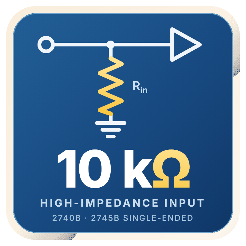
    • Impedance: 50 Ω (default) or 10 kΩ (personalization by ordering code) on single-ended inputs; 100 Ω on differential inputs

    • ICMR (Input Common-Mode Range): ± 12 Vdc referred to GND (Differential mode only)

    • Gain: x1 ÷ x100, software programmable in steps of 0.5 dB independently on each 16-channel group

    • Connector Type: 2mm 40-pin header male (input adapters available)

    • Full Scale Range: 4 Vpp

    • DC Offset: Adjustable in the ± 2.5V range independently on each input channel

    DIGITAL CONVERSION

    • Resolution: 16 bits

    • Sampling Rate: 125 MS/s simultaneously on each channel; scalable by 2n decimation factor (n = 1 to 10, Scope firmware only)

    SYSTEM PERFORMANCE

    • ENOB (Typ.): 12.0 (@5 MHz, -3dB, Gain x1)

    • RMS (Typ.): 3.6 LSB RMS (@Gain x1)

    DIGITAL I/O

    LVDS I/O

    TRG-IN/TRG-OUT/GPIO/S-IN

    • 16 differential pairs

    • Sw programmable I/O (individual self-trigger outputs, trigger validations, Veto, Busy, Start, Stop, Pattern Input, etc.)

    • LVDS

    • Zdiff = 100 Ω (when set as inputs)

    • 2.54mm 34-pin AMPMODU Mod II male connector

    • General purpose I/Os

    • Sigle-ended TTL/NIM

    • LEMO 00 male connector

    • Sw programmable (trigger, gate, veto, busy, etc.):

    • TRG-IN/S-IN internally terminated with 50 Ω (Zin = 50 Ω)

    • TRG-OUT requires Rt = 50 Ω

    • GPIO as Input must be terminated with 50 Ω

    • GPIO as TTL Output requires Rt = 50 Ω

    • GPIO as NIM Output requires Rt = 50 Ω or 25 Ω

    ANALOG OUTPUT

    • Sw programmable DAC output for signal inspection, pulse generation, majority level

    • 14-bit Digital-to-Analog Converter (DAC)

    • 125 MS/s Update Rate

    • LEMO 00 connector

    • ±1 V @ 50Ω load

    • ±2 V @ hi-Z load Output Range

    ACQUISITION MEMORY

    • 2.5 GB total DDR4 memory size (20.971 MS/ch) divisible in multiple buffers

    • Maximum record length: ≃ 84 ms @ 125 MS/s (total memory size divided by 2)1

    1 Value referred to the Scope firmware (minimum of two buffers admitted)

    TRIGGER AND EVENT ACQUISITION

    Triggered Mode

    Trigger Sources

    Trigger Timestamp – Scope firmware

    All the channels fire simultaneously upon a global trigger generated by the Central Logic Unit receiving the trigger source signals; a zero suppression function is available.

    • Software by register writing

    • External upon the leading edge of The TRG-IN signal (TTL/NIM)

    • Local (self-trigger) upon the channel discriminator with programmable threshold

    • Resolution: 8 ns coarse time stamp

    • Counter range: 48 bits

    • Full-scale range: ~625 h

    Streaming Readout Mode

    Each channel autonomously identifies the ROI and uses the local trigger to get events independently on the other channels; validation logics can be configured for correlated acquisition (coincidence/anticoincidence).

    Trigger Timestamp – DPP firmware

    • Resolution: 8 ns coarse timestamp, 8 ps fine timestamp

    • Counter range: 48 bits

    • Full-scale range: ~625 h

    SYNCHRONIZATION

    Clock Generation

    CLK-IN/CLK-OUT Connector

    By default, the Digitizer’s main clocks can be optionally generated upon the internal 50MHz or external 62.5MHz reference (CLK-IN). Onboard programmable PLL allows locking to different external frequencies.

    • Two differential pairs:

      – CLK, reference clock signal

      – SYNC, synchronization signal (start/stop, T0, etc.)

    • 2.54mm 4-pin AMPMODU Mod II male connector

    • CLK-IN: AC-coupled LVDS, ECL, PECL, LVPECL, CML (Zdiff = 100 Ω)

    • CLK-OUT: LVDS

    Clock Synchronization

    Default 62.5MHz frequency distributed by:

    • Fan-out to CLK-IN

    • CLK-IN/CLK-OUT Daisy chain with sw programmable CLK-OUT delay shift

    Custom frequencies can be supported upon request.

    Data Synchronization

    Programmable Busy/Veto logic on differential LVDS I/O, or single-ended NIM/TTL I/O for event building.

    Run Synchronization (Acquisition Start/Stop)

    Optionally, by Daisy chain or fan-out propagation through differential CLK-IN/CLK-OUT or LVDS I/O, or single-ended NIM/TTL I/O.

    Trigger Distribution

    TRG-IN/TRG-OUT NIM/TTL LEMO I/O (global trigger) or LVDS I/O (global or local trigger).

    FIRMWARE

    Firmware stored in the on-board Flash Memory and live rebootable by Web Interface

    DPP Firmware (Shareware)

    Scope Firmware (Freeware)

    Upgrades (Free)

    Pay firmware implementing a digital pulse processing algorithm:

    • DPP-PSD: Charge Integration, Pulse Shape Discrimination, CFD for fine timestamp

    • DPP-PHA: Pulse Height Analysis

    • DPP-ZLEplus: Zero Length Encoding

    30-minute per power cycle in Trial mode; license is required for full-time work.

    • Firmware for the waveform recording

    Designed for waveform recording.

    Web available CUP files for Scope and DPP firmware upgrade via Web Interface or CAEN Toolbox software.

    FPGA

    • Xilinx Zynq UltraScale+ Multiprocessor System-on-Chip mod. XCZU19EG

    • Processing System based on Quad-core Arm with 2GB DDR4 memory @2400 MT/s (Linux OS onboard)

    • Programmable logic with more than 1100K system logic cells and 80Mbit memory

    USER FIRMWARE (OPEN FPGA)

    SCI-Compiler

    User Firmware Generator and Compiler Graphical Tool for CAEN Programmable Boards.

    Scope Personalization

    DPP Personalization

    Customizable features of the Scope firmware:

    • Common trigger

    • Simultaneous waveform recording on 64 channels management

    • Trigger logic

    • Wave processing

    Customizable features of the DPP firmware:

    • Individual trigger and channel acquisition management

    • DPP algorithm

    • Trigger logic

    • Event data information

    COMMUNICATION INTERFACES

    1 GbE

    10 GbE (Contact CAEN Support)

    USB 3.0

    • Copper RJ45 or optical LC connector on SFP+ transceiver

    • TCP protocol

    • Transfer rate: 110 MB/s

    • Copper RJ45 or LC optical connector on SFP+ transceiver

    • UDP protocol

    • Transfer rate: 850 MB/s

    • USB-C type connector

    • USB 3.1 GEN1 protocol

    • Transfer rate: 280 MB/s

    SOFTWARE

    Readout SW for CAEN Firmware (Freeware)

    SCI-Compiler for Open FPGA (Shareware)

    • CoMPASS spectroscopy software (DPP firmware only)

    • WaveDump2 (Scope firmware only)

    Automatic generation of drivers (USB, Ethernet), libraries, and demo software for Windows®, Linux®.

    SDK and Tools (Freeware)

    General-purpose libraries (C/Python) with demo samples for host Windows® and Linux® PC, and embedded Arm.

    Web Interface

    Firmware management (e,g. upgrades and on-the-fly selection of the firmware to run), board information, PLL and Ethernet configuration, board status monitoring.

    ENVIRONMENTAL

    • Environment: Indoor use

    • Operating Temperature: 0°C to +40°C

    • Storage Temperature: -10°C to +60 °C

    • Operating Humidity: 10% to 90% RH non condensing

    • Storage Humidity: 5% to 90% RH non condensing

    • Pollution Degree: 2

    • Overvoltage Category: II

    • EMC Environment: Commercial and light industrial

    REGULATORY COMPLIANCE

    • EMC: CE 2014/30/EU Electromagnetic Compatibility Directive

    • Safety: CE 2014/35/EU Low Voltage Directive

    POWER REQUIREMENTS

    +12V: 1.4 A (Typ.)
    +5V: 9.0 A (Typ.)

    The values above are preliminary and referred to a 1-GbE Scope firmware; they are subject to change depending on the firmware type.

    Footer

    CAEN - Tools for Discovery Logo (RGB)

    CAEN S.p.A.

    PI 00864500467 | REA: LU 102690

    C.I.V.: 500.500€ | CDU A47Ø7H7

    CAEN Group logo (B&W)
    IMQ Certification
    Cyber Essentials Plus

    About Us

    • Company Profile
    • Our policy
    • Sales network
    • Innovative Projects
    • Careers
    • How to reach us

    Resources

    • Documentation
    • Accessibility Statement
    • Legal and Compliance
    • Certifications

    Applications

    • High Energy Physics
    • Astrophysics
    • Neutrino Physics
    • Dark Matter Investigation
    • Nuclear Physics
    • Material Science
    • Medical Applications
    • Homeland Security

    Support

    • Getting Started with MyCAEN Portal
    • Login / Register
    • Wishlist

    News

    • News

    Contact Us

    • Contact
    • Privacy Policy
    • Cookie Policy
    • Whistleblowing

    Copyright © 2026 CAEN S.p.A. All rights reserved. Website by Addiction

    ✕